This thread has been locked.

If you have a related question, please click the "Ask a related question" button in the top right corner. The newly created question will be automatically linked to this question.

TPS543A26: Power Section review for TPS543A26RYSR

Part Number: TPS543A26
Other Parts Discussed in Thread: UCD90320

Hi,

Currently, we designed using a TPS543A26 part for multiple voltage rail power generations. In this Buck converter, Enable pin mentioned as current driven logic and also in datasheet mentioned "if going to provide the external digital control to enable pin, need to configure as an open drain/collector."

In our circuit, power monitoring & sequencing IC UCD90320 LGPO pin connected to enable of TPS543A26 with pull-down of 10K. By default, we are configuring LGPO pins as low driving and will be enabled by one-by-one power rails.

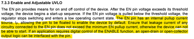
Our query is, whether it is mandatory to configure the enable pin as open drain in UCD90320?

It will impact any current driven issues? or pull down is suffient during OFF state?

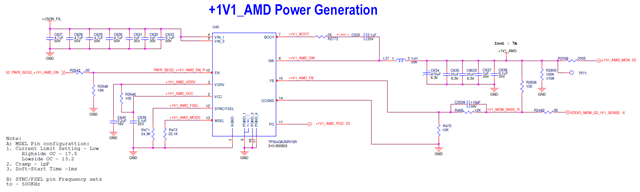
Also, Required your support to review the another Buck converter design. Please find the below DC-DC design for reference,

Thanks,

Dinesh

  • I need to review the enable question with someone from design.   My experience on the bench is it is okay to drive the enable pin. 

    I will review the schematic and give you feedback on Monday. 

  • Driving the enable is okay as long as the voltage is below the abs max voltage.

    Place a 1-μF/25-V/X6R or better dielectric ceramic capacitors from each VIN to PGND pins and place
    them as close as possible to the device on the same side of the PCB. Place the remaining ceramic input
    capacitance equal on both side of device next to these high frequency bypass capacitors.

    See figure 8-1 page 22 of datasheet for schematic example of agnd and pgnd connection and gosns connection

    See 8-23 page for pcb layout example.
    and 8.4.1 for layout guidelines.

    R470 and R468 andd C2509 should be near the U45 IC, see 8-23 for example pcb layout

    Connect AGND to PGND Use vias on the AGND islands on top layer to connect to AGND layer island on an internal layer. Connect the internal AGND island to PGND at one point.