Because of the holidays, TI E2E™ design support forum responses will be delayed from Dec. 25 through Jan. 2. Thank you for your patience.

This thread has been locked.

If you have a related question, please click the "Ask a related question" button in the top right corner. The newly created question will be automatically linked to this question.

LM26420-Q1: Calculations and design of my power circuit and device request for the Webench simulator

Part Number: LM26420-Q1
Other Parts Discussed in Thread: TPS62442-Q1, RM46L852, LM26420, LAUNCHXL2-RM46, PSPICE-FOR-TI

Hello, my name is Francisco, engineer of the R+D+i Department of Rother Industries & Technology company. I would like to verify the calculations made for my power circuit design using the LM26420Q1XMHX/NOPB DC/DC converter.

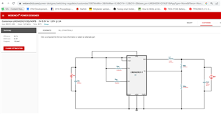
I attach the design of my power circuit.

To obtain V_OUT=3.3 V and Iout (max)=2 A:

V_IN=5 V, F_s=2.2 MHz

V_REF=0.8 V and R2=10 kΩ
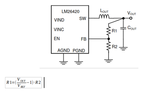
R1= 31.6 

I_LPK=2.4 A

Δi_L=0.2

D=3.3/5

T_s=1/fs=1/2.2 MHz=454.54 ns

L=0.64 μH -> 1 μH

To obtain V_OUT=1.2 V and Iout (max)=2 A:

V_IN=5 V, F_s=2.2 MHz

V_REF=0.8 V and R2=10 kΩ -> R1= 5.1 

I_LPK=2.4 A

Δi_L=0.2

D=1.2/5

T_s=1/fs=1/2.2 MHz=454.54 ns

L=0.52 μH -> 1 μH
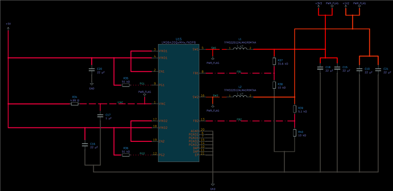
I use the following components:

The TFM322512ALMA1R0MTAA inductances of 1μH, the CL21A226KOQNNNG capacitor of 22 μF, the YR1B31K6C resistance of 31.6 kohm, the LR1F10K  resistance of 10 kohm, the H85K11BC resistance of 5.1 kohm, the MBA02040C4998FC100 resistance of 4.99 ohm, the LR1F51K resistance of  51 kohm and the B32529C0105J189 capacitor of 1 μF.

I have the problem that the output voltage has a lot of ripple. Therefore, I need to modify the values of the inductances and the output capacitors to reduce this ripple. However, the LM26420-Q1 is no longer available in the Webench simulator. Could you enable this device in the Webench simulator to develop my LC low pass filter using this inductance and output capacitors?

Best regards,

Francisco.

  • Hi Francisco,

    Thanks for reaching out to us.

    First, we have a new dual buck (TPS62442-Q1) that you might like to consider as it will offer better efficiency and thermal performance due to lower RDSon and smaller solution size (smaller IC footprint).

    The schematic diagram looks fine. I'm just curious about the ripple voltage spec and actual ripple in your application. Can you share this data including the ripple voltage waveform?

    By the way, you can still use the Webench simulator by opening the link below. Let me know if you are able to use it.

    https://webench.ti.com/power-designer/switching-regulator/customize/196?VinMin=3&VinMax=5.5&O1V=1.2&O1I=2&base_pn=LM26420X-Q1%2F1&AppType=None&Flavor=None&op_TA=30&origin=pf_panel&lang_chosen=en-US&optfactor=3&Topology=Buck&flavor=None&VoltageOption=None

    Best regards,

    Excel

  • Hi Excel Regidor,

    Currently, I will continue using the LM26420Q1XMHX/NOPB DC/DC converter for my first prototype version. If the TPS62442-Q1 DC/DC Converter complies my objectives, I will replace the LM26420Q1 in my second prototype version, which will be applied IoT technology.

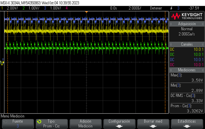
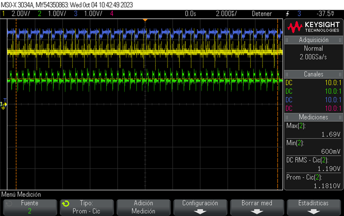
    I attach the current ripple voltage:

    The yellow signal corresponds to the input voltage of 5 V. As you can see the LM26420Q1 causes a distortion on this input. I generate this signal with a power supply called RSPD 3303C. However, for my application circuit I will generate the input signal through the TEN 8-2411WI DC/DC Converter, I still have not checked if with this DC/DC converter the LM26420Q1XMHX/NOPB DC/DC could generate this distortion.

    The blue signal corresponds to the input voltage of 3.3 V. The ripple voltage corresponds to the output of 3.3 V, it has a maximum of 3.58 V, RMS of 3.33V and a minimum of 2.89 V.

    The green signal corresponds to the input voltage of 1.2 V. The ripple voltage corresponds to the output of 1.2 V, it has a maximum of 1.69 V, RMS of 1.19V and a minimum of 600 mV.

    I obtain these signals when I connect, as a load, a resistor of 23. 7 Ω to the 3.3 V output and a resistor of 23.7 Ω to the 1.2 V output. However, the final load of my first prototype is the RM46L852 microcontroller and the devices that it controls.

    Therefore, I will have a current of 360 mA on the 1.2 V output voltage, I will have a current of 468 mA on the 3.3 V output voltage and I will have a current of 237 mA on the 5 V output voltage for my first prototype version. However, in my second prototype (IoT implementation), the current draw on the 3.3 V and 5 V outputs.

    I need to get a maximum of 3.4 V and a minimum of 3.2 V for the 3.3 V output and a maximum of 1.3 V and a minimum of 1.1 V for the 1.2 V output. For these reasons, I have thought about modifying the values of the output inductors and capacitors to obtain an LC filter that provides a fc=7.3 using a capacitor of 100 uF and a inductor of 4.7 uH at each output. I will like to simulate this situation in the Webench simulator before doing any tests.

    The link that you sent me does not work. Does it work for you? It is essential to have this simulator.

    Best regards,

    Francisco.

  • Hi Francisco,

    First, how did you capture the voltage waveforms? Did you use the tip and barrel method (see figure below)? You refer the app note below for details.

    (https://www.ti.com/lit/an/slvaf30/slvaf30.pdf?ts=1696494544803&ref_url=https%253A%252F%252Fwww.google.com%252F)

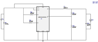
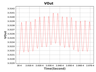
    Yes, Webench simulator is working. See the simulation result below for the 3.3V output. I also attached the simulation result.

    Schematic diagram:

    Vout ripple:

    WBDesign197_Steady State-1.pdf

    Can you open the link (https://www.ti.com/product/LM26420-Q1) and click the "Open design" menu. It will open a new window for the Webench Power Designer.

    Let me know if you are available to open the simulator.

    Best regards,

    Excel

  • Hello Excel Regidor,

    I have used both the tip and barrel method and the classic method. I am doing the tests on breadboards and this situation affects the behavior of the signals. However, it should not cause too many voltage ripples.

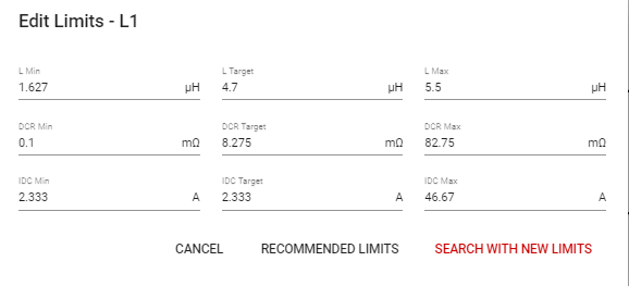
    Yes, I can. Thanks. I have verified that obtaining a 3.3 V output the recommend value of inductor should be greater than 1.627 H and less than 3.702 H and its internal resistor should be greater than 0.1 mΩ and less than 82.75 mΩ. Why? In what section of the document do the calculations appear to obtain these results? I need to document all of these aspects.

    Best regards,

    Francisco.

  • Hi Francisco,

    Thanks for the updates.

    Can you send the simulation result so I can check why the recommended DCR value is too low?

    Best regards,

    Excel

  • Hi Excel,

    I attach you the simulation design and its results.

    On the other hand, I would like to know the equations and calculations that the simulation does to obtain these results. I need this information to design my circuit because I have verified that a decrease in the current causes an increase in the inductance of the inductor. For this reason, I think that this relationship is the phenomenon that causes this anomaly. So, I think developing an LC filter that provides a fc=7.3 using a capacitor of 100 uF and a inductor of 4.7 uH at each output should resolve this problem.

  • Hi Francisco,

    Thanks for the sharing the simulation result.

    On the figures above, the inductor value is 2.2uH for both output rails. Where did you got the 1.627H (min) / 3.702H (max)? Are they typo errors? Should it be 1.627uH / 3.702uH?

    The recommended limits indicated in the Webench works in most application (see figure below). And it can be modified based on your preference. You can simulate the effect of having a 4.7uH inductor and 100uF output capacitor. See the example below.

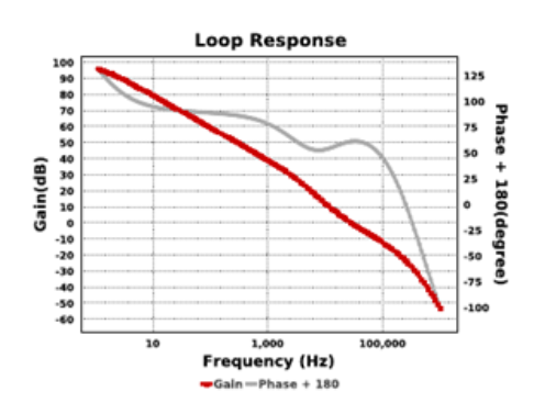
    Just ensure that is has stable loop response by checking phase ( >= 45 deg. ) and gain (>=10dB) margins.

    Anyway, the formulas to calculate for the inductance was already indicated in the datasheet. The only difference is the k factor (0.058 to achieve a 2.2uH inductor), which is 0.1 to 0.2 equation 11. 


    I hope I was able to address your queries.

    Best regards,

    Excel

  • Hi Excel,

    Yes, they are typo errors.

    Yes, I know that the LM26420-Q1 datasheet appears the equations and calculations about the value of the inductor and capacitance. However, the minimum and maximum values required are not detailed, but in the simulator they are detailed and that is the question I am requesting.

    On the other hand, Where in the webench simulator can I see the values of the phase and gain?

  • Hi Francisco,

    Apologies for the late response.

    You can set the k-factor in the equation below to 0.12 and 0.052 for the minimum and maximum inductance, respectively. For the minimum and maximum Cout, it was set by the IC designer to ensure stable control loop.

    The file you attached already contains the bode plot simulation. See figure below.

    Best regards,

    Excel

  • Hi Excel,

    You should know that an information without its explanation and its source is useless. If you remember, I wrote the calculations according to the datasheet at the beginning of this post. Therefore, I already know the equations of the datasheet. The problem is that if I apply this calculated values I experience the anomaly that I have detailed in this post. The other problem that I have commented is that these values have not related to the recommended values by the Webench simulator. For this reasons, I want to know the equations that apply the simulator or is it simply that this simulator only serves to waste my time.

    On the other hand, the parameter that you call k refers to the desired ripple tolerance in the current. This tolerance is 20 % for this reason its value is 0.2. Regarding the values 0.12 and 0.052. From what source or website did you get it?
    These values do not appear specified in the datasheet and do not make sense with respect to the maximum and minimum values of the simulator since if the maximum corresponds to 2.2 uH (L=(D·T_s)/(2·∧i_L)=((3.3 /5)·454.54·10⁹)/(2·0.058·2)) why 3.7 appears as the maximum recommended value in the simulator for an input voltage of 5V and an output of 3.3 V and 2 A and why doing the calculations according to the datasheet for k=0.2, the value 0.64 uH is obtained as the nominal inductance. Does this imply that it would not be possible to use a value greater than 2.2 uH to obtain a higher cut-off frequency?
    Please, I would appreciate it if you could answer these questions clearly, I have been debating this for several days and I still have not received a good answer.

  • Respect to your response, I have three questions:

    1. Does the bode diagram attached to the report represent the frequency response of Vout vs Vin? I don't see any information about these parameters in the WEBENCH simulator.

    2. In which source or section of datasheet is defined the >=45º and >=10dB rule? Is this rule related to the frequency cut-out point?

    3. How I can see from this graphic that this rule is followed? What points on the graph represent this situation?

  • I have tried different values of inductance (4.7 uF) and capacitors (100 uF) and the problem persists. Could anyone else help me with this problem?

  • Hello Francisco,

    Apologies for the late response.

    Give a few hours and will respond to your queries.

    Best regards,

    Excel

  • Hi Excell, I am currently quite disappointed with Texas Instrument and its product. I can't understand the causes that cause this anomaly when the calculations are correct. With so many modifications and tests, I have spent a considerable amount of money compared to the cost of this type of converters and, above all, a great waste of time.

  • Hi Francisco, 

    The Webench model for LM26420-Q1 is not fully optimized so it doesn't give an accurate simulation results. Anyway, the limits for the passive component values (Cout, Lout) can be manually adjusted. Unfortunately, I cannot make a screen shots because the Webench is not working properly now. I will provide you a detailed instruction on how to do it so you can simulate your desired values (L = 4.7uH, Cout = 100uF).

    With regards to the ripple issue, it's not clear for me what causes it. Can you share a waveform with SW voltage, inductor current, VIN and VOUT? There might be unstable switching cycles generating high ripple. I also suggest to buy an EVM (see link below) so you can check it's behavior compared to your board at the same application condition.

    By the way, can you share PCB layout as well?

    Best regards,

    Excel

  • Hi Excell,

    I attach the design of my power circuit that I am using in my tests.

    1º I simulate the power circuit for a resistance of 23.7 ohm.

    2º I simulate the power circuit for a resistance of 3.3 ohm

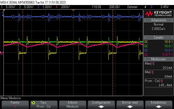
    In the first test, I obtain the following behaviors:

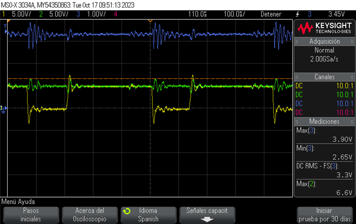
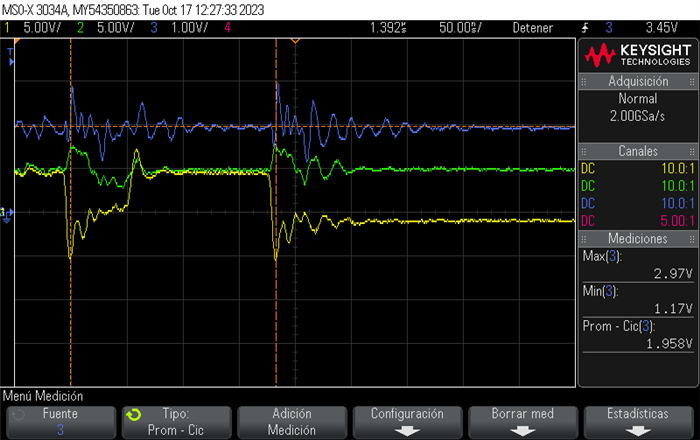
    The yellow signal corresponds to the SW1, the green signal corresponds to the power input of 5V and the blue signal corresponds to the output signal of 3.3 V. I generate this power input with a power supply called RSPD 3303C.

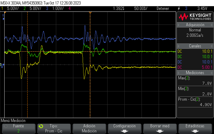
    As you can see the LM26420Q1 causes a distortion on the power input and output signal when it switches. This commutation causes a maximum voltage peak of 3.90 V and a minimum voltage peak of 2.65 V for the output signal, both situations are very negative for my components.

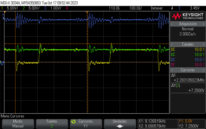
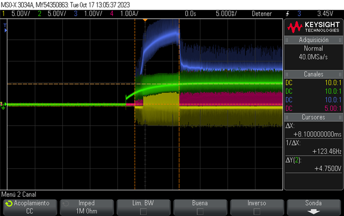
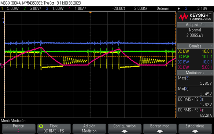
    The signal references correspond to the previous case. As you can see the LM26420Q1 switches to the appropriate frequency, that is, 2.2 MHz. In addition, you can see that the power input reaches a voltage of 7,25 V.

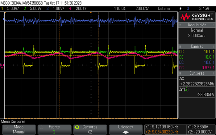
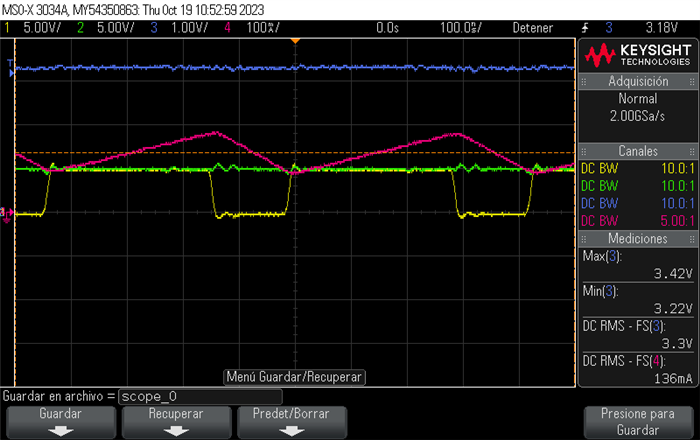
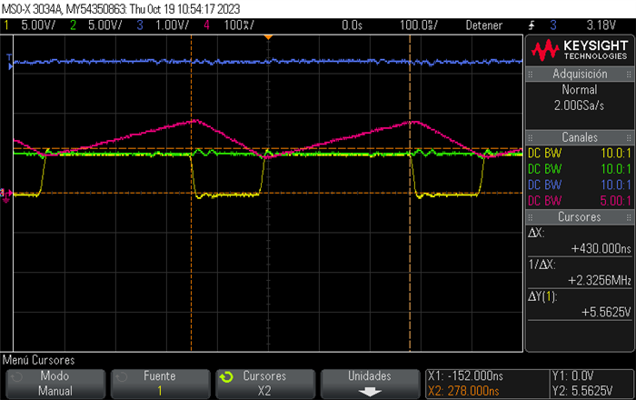
    The yellow signal corresponds to the SW1, the green signal corresponds to the power input of 5V, the blue signal corresponds to the output signal of 3.3 V and the red signal corresponds to the inductor current. You can see that the DC/DC Converter is switching correctly. In addition, the value of the current (It is measured with the N7206 current probe of Keysight) is similar to the value calculated, that is:

    Iout=Vout/R=0.139 =139 mA approximately 145 mA

    L=((D·T_s)/(2·∧i_L))·(V_in-V_out) -> ∧i_L=(D·T_s·(V_in-V_out))/(2·L)=((3.3/5)·454.54·(10^-9)·(5-3.3))/(2·4.7·(10^-6))->∧i_L=0.054-> ∧i_L=k·Iout->k=0.054/0.145=0.37 -> 37% of ripple current. Therefore, I_LPK=I_out+∧i_L-> I_LPK=0.145+(0.37·0.145)=0.19865 approximately 200 mA.

    Although the behavior of current appears correct, the behavior of the input and output voltage is dangerous.

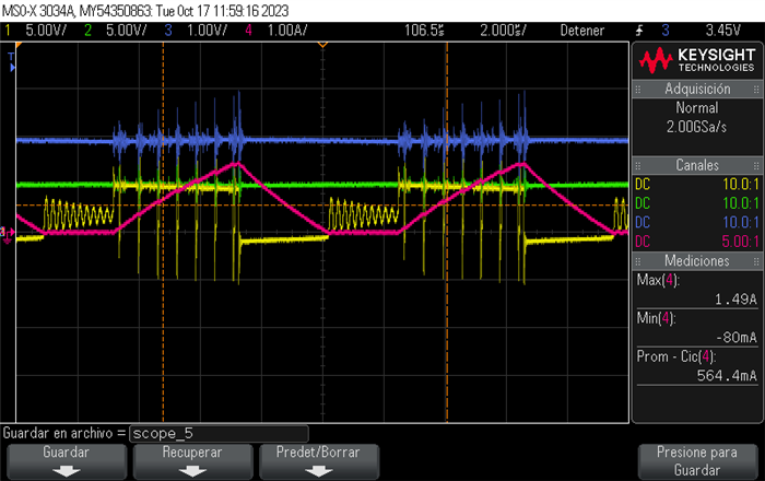
    In the second test, I obtain the following behaviors:

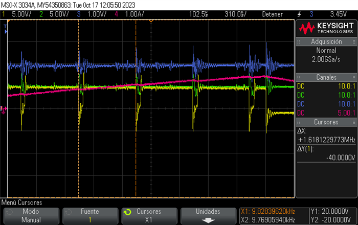
    The signal references correspond to the previous case. As you can see the DC/DC Converter enters the discontinuous conduction mode continuously and the LM26420 is unable to perform the switch correctly.

    In addition, you can see that this Converter is unable to work to the appropriate frequency and It can only operate at a frequency of 1.6 Mhz.

    In addition, you can see that the power input reaches a voltage of 7,8 V. It is too high a value

    On the other hand, you can see that this situation causes a decrease on the value of the output voltage.

    At first, the DC/DC converter tries to work correctly and reach the output of 3.3 V, but when the power input reaches a value close to 5V, it therefore enters the discontinuous conduction mode.

    At this time, I do not want to buy EVM because I have already invested too much money in the modifications made to the LC circuit and since I am experiencing abnormal behavior in this converter and have not yet obtained an acceptable approach or explanation about this, I do not wish to invest more money at the moment in this product.

    Best regards,

    Francisco.

  • As I mentioned in the conversations at the beginning, I am testing the device on breadboards before developing its printed circuit board. Do you want me to take a photo of them?

  • Hi Francisco,

    Thanks for the detailed updates.

    I have few questions to understand the issue better.

    1. What's the oscilloscope bandwidth when you measured waveforms? Can you re-measured it again at 20MHz bandwidth?

    2. What is the difference between 1st (stable waveforms) and 2nd (unstable waveforms) test? Is it the resistor load?

    3. Can you share the photo of your board setup and how you are measuring the voltage waveforms?

    Best regards,

    Excel

  • Hi Excel,

    Apologies for the late response. Yesterday I was in a meeting of great importance for the company and of special scope.

    1. The oscilloscope bandwidth for the previous images is 350 MHz. Yes, I have configured the oscilloscope bandwidth for this frequency and I get a better measured.

    In the first test, I obtain the following behaviors (resistance of 23.7 ohm):

    The yellow signal corresponds to the SW1, the green signal corresponds to the power input of 5V, the blue signal corresponds to the output signal of 3.3 V and and the red signal corresponds to the inductor current.

    As you can see the distortion, that the LM26420Q1 causes during the switching, is negligible. The value of the current is practically the same as the theoretically calculated value.

    In the second test, I obtain the following behaviors (resistance of 3.3 ohm):

    The yellow signal corresponds to the SW1, the green signal corresponds to the power input of 5V, the blue signal corresponds to the output signal of 3.3 V and and the red signal corresponds to the inductor current.

    As you can see the anomaly persists (Since digital filtering due to bandwidth reduction only affects the acquisition of the measurement).

    2. Sorry, I haven't put it in detail. The first test corresponds to the resistance of 23.7 ohm and the second test corresponds to the resistance of 3.3 ohm.

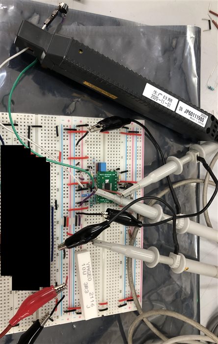
    3. I attach you the image of my power circuit on the breadboards:

    Once all these issues have been analyzed, I can hypothesize that this anomalous behavior must be related to its development in a breadboard, an issue that only affects when high-frequency switching occurs. These switching causes very high peaks at the power input, which results in distortions in the output voltage. When a load that consumes a lot of current is applied, the switching causes higher peak values, exceeding the overvoltage limit of the LM26420, this results in the device entering discontinuous conduction.

    However, my final product, that is, once these tests on the breadboard have been passed, the circuits will be implemented on a PCB. Therefore, much of this anomaly will be overcome. However, my final product will be subject to EMI interference and must comply with MIL-STD regulations, so there will be interference that affects the power input and this behavior will occur again.

    In conclusion, the solution that I propose is to use an LC filter at the power input as well as the application circuit against EMI interference that the manufacturer TDK specifies for its PXB15-24WS05/NT DC/DC Converter.

  • Hi Francisco,

    Breadboard is not ideal for evaluating switching converters because the high parasitic capacitance and inductance created by the long wires can heavily influence the device behavior especially at higher load current. So, I still suggest to order an EVM and do a detailed evaluation before implementing your solution in the actual PCB.

    Placing LC filter on the input and output rails can mitigate the high frequency noise. You can refer to the app notes below for designing input and output filters.

    Input filter design: https://www.ti.com/lit/an/snva801/snva801.pdf?ts=1697717901358&ref_url=https%253A%252F%252Fwww.google.com%252F

    Output filter design: https://www.ti.com/lit/an/snva871/snva871.pdf?ts=1697716350257&ref_url=https%253A%252F%252Fwww.google.com%252F

    Do you have additional queries?

    Best regards,

    Excel

  • Hi Excel Regidor,

    I understand your interest in purchasing the EVM, but I would like, first of all, to be able to make the most suitable input and output LC filter. Because I am totally sure that there will be no problem with the EVM board, just as there is with the LAUNCHXL2-RM46. However, in my final device, I must consider that such interference may occur, which I have been able to verify poses a risk to the health of my device.
    With the data that I have provided about the voltage peaks produced, could you provide me with the most appropriate input and output LC filter and its explanation? Would it be possible to provide me with the model of those LC filters along with the LM26420 for your PSPICE-FOR-TI program?
    Best regards,
    Francisco.

  • Hi Francisco,

    The main reason I'm recommending you to have an EVM is to determine if you still need an input and output LC filter in your application.

    For input and 2nd filter designs, you can use the attached calculation tools to determine the LC filter values.

    Unfortunately, we don't provide models for LC filters. You can check the manufacture's website for the models.

    2703.InputFilterCalculator.xls

    2ndStageFilter_Equations.xls

    Best regards,

    Excel

  • Hi Excel,

    I will purchase the EVM. However, firstly I would like to understand the LC filter needed for this DC/DC Converter. Then, when I have the best LC circuit for this worst situation (breadboard), I will extrapolate it to PCB, that is, EVM circuit. Finally, with this data I will can manufacturer my PCB with complete safety.

    On the other hand, there is a misinterpretation. I am not going to buy an LC filter IC.

    I was referring to whether you could provide me with the design of the LC filters, which you gave me in the Excel files, along with a disturbance source in a PSPICE file for the PSPICE for TI program. The reason lies in the need to obtain Bode plots.
    Best regards,
    Francisco.

  • Hi Francisco,

    In most application, LC filters are not required. Do you have specs on the input and output noise level? What is the end equipment for this project?

    On other hand, you cannot use your current circuit as a reference for designing the LC filter and scale down it later once you have your PCB because there's too much noise into it.

    I think the best approach is to evaluate the EVM first. Then, assess if you need an LC filter to meet the ripple/noise requirement spec of your application. Use the calculation tool to design LC filter. Implement it filters into the EVM and perform bode plot measurements.

    Let me know your thoughts.

    Best regards,

    Excel

  • Hi Excel,

    I would ask you not to insist on the EVM board, I find it abusive. The solution I intend to achieve and how it has been demonstrated is the need for input and output filters. I have told you that I will acquire this board, but as you can understand throughout my explanations, I would like to have an LC output filter with a cutoff frequency of 7.33 (in my case I have tried to obtain it with an inductor of 4.7 uF and a 100 uF capacitor).

    Therefore, such a filter is not implemented on said board. That does not mean that I do not intend to use it, simply what I am asking is the way to be able to virtually simulate these issues, that is, the correct functioning of the filters and then physically implement them on the EVM board, on the breadboards and in a simple PCB that I am developing. Therefore, I would like to ask you, as I mentioned in the previous message, that you will please pass me the input and output filter circuit along with an input signal that generates disturbances and the LM26420 for the PSICE for TI program, since it is more feasible and easier for me to be able to visualize all these issues in a virtual simulator.

    On the other hand, you have only given me a version of an LC filter with an electrolytic capacitor for the input voltage. Could you give me an LC filter with such features for the output?

    The objective is to comply with the MIL-STD 810 specification for interference and vibration. My application is specifically for the automotive sector but applicable to the industrial sector and a special one that I would not like to specify (you can imagine which one it is since I have to comply with the MIL-STD regulations). Therefore, it is a priority in my field, unlike most others, to design input and output filters.

  • Hi Francisco,

    Unfortunately, we don't offer any type of model for LM26420 because it's a very old device. For the passive components (ferrite bead and capacitor), kindly check with vendor to get an accurate models.

    On the other hand, the input filter calculator can be used with ceramic capacitor as well (see attached file). Typically, damping resistor is not needed when ferrite bead is used. Just need to perform input and output impedance plot to ensure no resonance peaks.

    InputFilterCalculator_BLM21SP700SH1.xls

    Best regards,

    Excel

  • Hi Excel, 

    Thanks for your reply. In my previous question, I was referring to whether the input LC circuit (coil, electrolytic capacitor and ceramic capacitor) that you gave me was also applicable to the output. Would it be applicable or not?

    On the other hand, it is very strange your reply. The only thing I ask now is a schematic of the LC filter that you have recommended to me for the LM26420 converter along with a disturbance source at the filter input simply to study and be able to decide according to my choices which components to use, the values of those components and be able to make a comparison of this virtual simulation with the physical tests obtained from the breadboards, EVM and the PCB for testing.
    The schematic or model that I request is for TI application called PSPICE for TI, which does include the LM26420 component in its libraries (A question that I do not understand why you say no to me, when you can even download different simulation models from your website: www.ti.com/.../LM26420. For this model or schematic, at no time have I asked or demanded that Texas Instrument tell me which LC filter IC I should choose or that Texas Instrument tell me which manufacturers and references should be chosen to form the LC filter, these are conclusions drawn and misinterpreted. The only thing I am asking for, just like what you offer in the Design tools & simulation section of the LM26420 website, is a model made up of the generic coil, generic electrolytic capacitor and generic ceramic capacitor (LC Filter) (both components are already defined in the PSICE for TI program), by the LM26420 (already included in the libraries although it is in its reduced single-channel version) and finally a continuous voltage source together with a voltage source that simulates a possible disturbance. 

    If the problem is that you or its team of engineers do not know how to use this tool, please have a colleague from Texas Instrument who knows how to use the PSPICE for TI program help you with this matter. Because the only thing I ask is that the same thing that you have sent me in an Excel file, I would like to have it in this program so I can simulate it in detail and virtually.

    Best regadrs,

    Francisco.

  • Hi Francisco,

    First, there is no LM26420-Q1 model, but you can use the LM26420 (non-automotive) Pspice model for simulation.

    Can you kindly confirm if the sample schematic with input LC filter with voltage source for noise disturbance below is enough (in red)? I will add the 2nd stage LC filter on the output if this is what you need.

    Best regards,

    Excel

  • Hi Excel, thanks for you reply.

    Apologies for the late response. Yesterday I was in a meeting of great importance for the company.

    This is exactly what I was asking. It would only be necessary to add the 5V direct voltage source at the input before the disturbance and I suppose that the C4 capacitor should be electrolytic according to the document you sent me.

    Best regards,

    Francisco.

  • Hi Francisco,

    Please see the attached model and let me know if it runs.

    The values indicated in the LC filter on input and noise source (V1) are an example only. Kindly redesign it according to your requirements.

    C4 should be a ceramic capacitor with low ESR as it use to suppress the high frequency noise coming from the VIN pin of the IC.

    Best regards,

    Exce

    lLM26420X_PSPICE_TRANS.zip

  • Hi Excel,

    Thanks for your help.

    Ok, I will redesign the input power source. Thanks for the information of C4 capacitor, I understand that you have done it.

    I am going to test the file that you sent me and then let you know that it works correctly.

    Best regards,

    Francisco.

  • Hi Excel,

    I am testing the device in different situations (protoboard, EVM board and PCB for testing) and I have realized a detail that is specified in the LM26420 datasheet and I would like confirmation that it is true. The following information appears on page 33:

    Copper planes dedicated to ground play a fundamental role in signal quality. On the other hand, for the GND connection the GND signal closest to the DAP pins must be used (all PGND1, PGND2, DAP, etc. signals are interconnected to the same ground plane, but the signal quality is better on the DAP pins). I have been able to verify that the signal quality improves considerably with the use of these copper planes as well as taking the GND as close to the DAP pins. Could you offer me your opinion on this?

    Best regards, 

    Francisco.

  • Hi Francisco,

    Can you share the initial PCB layout/connection and with the improve signal quality (GND as close to the DAP pins) to better understand the difference between the two layouts?

    Best regards,

    Excel

  • Hi Excel,

    Apologies for the late response, right now I'm very busy. This week I send you the information.

    Best regards,

    Francisco.

  • Hi Francisco,

    Just a gentle reminder.

    Can you share the initial PCB layout/connection and with the improve signal quality (GND as close to the DAP pins) to better understand the difference between the two layouts?

    Best regards,

    Excel

  • Hi Excel,

    Apologies for the late response. Currently, I am verifying the calculations because I have detected a typo in the LM26420-Q1 datasheet. When I finish, I will comment you all these aspects.

    Best regards,

    Francisco.

  • Hi Francisco,

    Just a gentle reminder. Is your issue already resolved? 

    Looking forward on your feedback.

    Best regards,

    Excel

  • Hi Excel,

    I have finished. Apologies for the late response. Firstly, I was studying in detail the behavior of the Buck DC/DC Converter. Secondly I applied this learned knowledge to the LM26420-Q1 datasheet and I detected typos. Finally, I verified the PCI design again that I have developed.

    I would like to comment on a brief conclusion of this study. The following picture shows the relationship between ripple voltage and ripple current with the parameters of the DC/DC Converter, in steady state.

    In the case of the LM26420-Q1, the Ts or fs parameter is a fix value and it is 2.2 MHz. Therefore, the user only can control the ripple voltage and the ripple current via the capacitor and the inductor of the LC circuit. The ripple current is directly related to the inductance and the ripple voltage is directly related to the capacitance and indirectly related to the inductance through of the ripple current.

    So, it has got an typo in the LM26420-Q1. The following picture shows this typo:

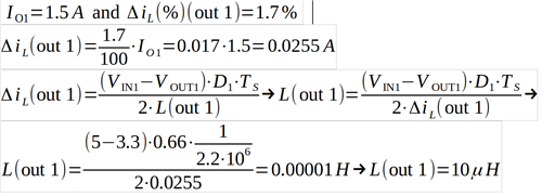
    • The first objective is to obtain:


        Therefore, the variation range of the output current will be:


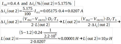
    • The second objective is to obtain:


        Therefore, the variation range of the output current will be:


    In the data sheet, it is commented that the value of the capacitor affects the stability of the transient  state. Could you provide me with more information about this aspect? Could you provide me with information about the transient state process performed by the LM26420-Q1, I can't find much information about this aspect in its datasheet?

    Tomorrow, I am going to post the design of my PCB, I need to dedicate some time to reference and explain it so that it can be understood correctly, given that I use various copper planes and follow the steps to comply with the recommendations defined in the datasheet. I would like you to verify that these steps comply with these recommendations.

  • Hello again Excel,

    Below I detail the methodology carried out in the copper track routing process.

    Schematic:

    PCB Design:

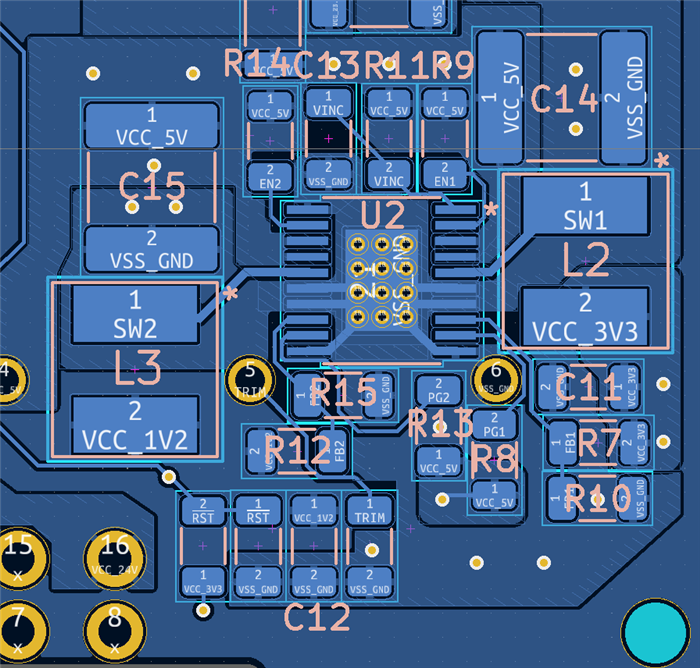
    • VSS_GND signal: This signal has got mini-planes of copper in the bottom layer "B.CU" (LM26420-Q1 is located in this layer). In addition, the GND signal has an internal plane for it called IN1.CU
    • VCC_5V signal: This signal has got mini-planes of copper in the bottom layer "B.CU" (LM26420-Q1 is located in this layer). In addition, the 5V signal has an external plane for it called F.CU
    • VCC_3V3 signal: This signal has got mini-planes of copper in the bottom layer "B.CU" (LM26420-Q1 is located in this layer). In addition, the 3.3V signal has an internal plane for it called IN2.CU

    • VCC_1V2 signal: This signal has an external plane for it called B.CU

    According to the recommendations specified in the LM26420-Q1 datasheet.

    1º The distance between each input capacitor "C_IN" with its corresponding PGND pin is <12 mm. The  VSS signals of each "C_IN" are connected to the VSS_GND plane through of 2 plated vias near of these connections.

    2º The distance between each output capacitor "C_OUT" with its corresponding PGND and VIND pins is <12 mm.

    3º I am not sure complying this rule: There must be a continuous ground plane on the bottom layer of a two-layer board except under the switching node island. Because I have an internal plane for the GND signal that is placed on top of the LM26420-Q1 (this device is located on the layer below). Therefore, this internal plane is located above the copper trace of the SW1 and SW2 signals.

    4º The distance of the copper track of each FBx is short.

    5º The distance between each FBx signal with its corresponding resistors is <7 mm.

    6º The distance between the V_OUT_1V2 resistor with its corresponding inductor is  ≅6 mm (I don't know if it will be enough) and the distance between the V_OUT_3V3 resistor with its corresponding inductor is ≅ 7 mm.

    7º The tracks of the SWx are short and wide. The inductors chosen are shielded.

    8º No signals of the LM26420-Q1 are connected through of vias.

    I would appreciate it if you could confirm to me if these decisions made are correct.

    Below the copper layers of my PCB:

    Best regards,

    Francisco.
  • Hi Francisco, 

    Thanks for your feedback.

    Inductor alone does not define the output ripple voltage but have a major contribution on it, as shown in the formulas below. For the other statement in red, I cannot any issue with it. Can you elaborate on it?


    The output capacitor affects the crossover frequency of the control loop. And a higher crossover frequency will result to faster transient response, in return lower undershoot and overshoot. However, pushing the crossover frequency too high could create output voltage oscillation due to low phase margin. Anyway, this item can be verified by performing bode plot measurements and verifying the output voltage waveform during step load.

    I hope I was able to address your queries.

    Best regards,

    Excel 

  • Hi Excel,

    I have marked this sentence in red because it is a typo. As I mentioned before, the ripple current is directly related to the inductance and the ripple voltage is directly related to the capacitance and indirectly related to the inductance through the ripple current. Therefore, the sentence should be:

    The inductor value determines the output ripple current and the capacitor and inductor determine the output ripple voltage. Smaller inductor values decrease the size of the inductor, but increase the output ripple current and therefore the output ripple voltage. An increase in the inductor value decreases the output ripple current.

    One must ensure that the minimum current limit (2.4 A) is not exceeded, so the peak current in the inductor must be calculated. The peak current (ILPK) in the inductor is calculated by:

    Regarding the question I asked related to the capacitor and its effect on the transient state. Specifically, I would like to visualize along with a detailed explanation how the LM26420-Q1 behaves. This visualization can be done in the SPICE for TI simulator. However, I would like to ask if you could provide me a document that details the control loop and the different responses that the LM26420-Q1 makes to achieve stability under constant load and possible load variations.

    On the other hand, you have not yet given me feedback on the process I have gone through in my PCB design to comply with Texas Instrument's recommendations.

    Best regards,

    Francisco.

  • Hi Francisco,

    Thanks for the suggestions on the datasheet. We will look into it.

    We cannot share the details of the control loop because it is proprietary. Hence, the loop stability can be verified via AC analysis simulation or bode plot measurements.

    By the way, I apologized for the delayed response on the schematic and PCB layout. I will write a separate message to address your queries.

    Best regards,

    Excel

  • Hi Francisco,

    Please see my comments on schematic diagram and PCB layout below. You can also refer to the User's Guide for PCB layout recommendation. 

    User's Guide: (https://www.ti.com/lit/ug/snva353b/snva353b.pdf?ts=1703780087040&ref_url=https%253A%252F%252Fwww.ti.com%252Fproduct%252FLM26420-Q1%253FkeyMatch%253DLM26420-Q1%2526tisearch%253Dsearch-everything%2526usecase%253DGPN-ALT)

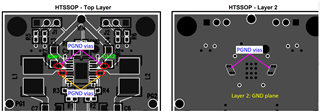
    In addition, you can also add power GND vias to reduce the parasitic inductance between PGND pins of the IC and passive components as shown below.

    1º The distance between each input capacitor "C_IN" with its corresponding PGND pin is <12 mm. The  VSS signals of each "C_IN" are connected to the VSS_GND plane through of 2 plated vias near of these connections. --> It looks fine.

    2º The distance between each output capacitor "C_OUT" with its corresponding PGND and VIND pins is <12 mm. --> It looks fine.

    3º I am not sure complying this rule: There must be a continuous ground plane on the bottom layer of a two-layer board except under the switching node island. Because I have an internal plane for the GND signal that is placed on top of the LM26420-Q1 (this device is located on the layer below). Therefore, this internal plane is located above the copper trace of the SW1 and SW2 signals. --> It means the next layer where the IC is placed should be a ground plane, which is the case in your PCB layout. So, I don't see any concern.

    4º The distance of the copper track of each FBx is short. --> It looks good.

    5º The distance between each FBx signal with its corresponding resistors is <7 mm. --> It looks good.

    6º The distance between the V_OUT_1V2 resistor with its corresponding inductor is  ≅6 mm (I don't know if it will be enough) and the distance between the V_OUT_3V3 resistor with its corresponding inductor is ≅ 7 mm. --> It is ok.

    7º The tracks of the SWx are short and wide. The inductors chosen are shielded.  --> It is ok.

    8º No signals of the LM26420-Q1 are connected through of vias. --> That's good.

    Best regards,

    Excel

  • Hi Excel,

    It saddens me to know that, but it is totally understandable. Therefore, the only way is how you say, that is, AC analysis simulation and bode plot.

    Best regards,

    Francisco.
  • Hi Excel,

    Thank you for your comments, I am happy to know that everything is correct.

    I am going to carry out the advice you have given me, that is, add power GND vias to reduce the parasitic inductance between PGND pins of the IC and passive components.

    Best regards,

    Francisco.

  • Hi Francisco,

    You're welcome. 

    If you don't have further queries, I will close this thread. You can re-open the thread by posting a comment or opening a new thread anytime.

    Best regards,

    Excel