This thread has been locked.

If you have a related question, please click the "Ask a related question" button in the top right corner. The newly created question will be automatically linked to this question.

BQ79616-Q1: Facing EMI issues

Part Number: BQ79616-Q1
Other Parts Discussed in Thread: BQ79656-Q1

Dear Team,

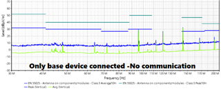
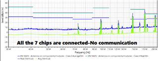
I am using BQ79616-Q1 in my BMS PCB.  All the functionalities are working as we expected. But the problem is its failing in EMI test (CISPR-25). My observation is that for every 25Mhz frequency(periodic), noise amplitude is shoot up 30dbuV/m to 40dbuV/m. 

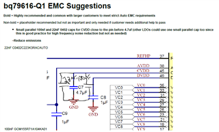
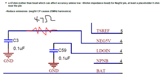
1. Can you tell me clock frequency/switching frequency using in chip. 

2.If you have any suggestions on to solve the problem, please share. 

  • Hello,

    Let me check with my design team and get back with you. Can you please explain your setup. Are you using a base device? How many 616 devices? Are the devices communicating?


    Thanks,

    chase

  • Hi,

    I am using six Bq79616-Q1 and one Bq79656-Q1. Total seven IC's. These are in stacked in series to achieve the required load voltage. 

    Here, Bq79656-Q1 is base device and Bq79616-Q1 is connected one above the other.

    Yes, we have conducted testing both with & without communication. 

    Sharing the waveform below for more understanding.

    above test repeated to higher frequency also, same shoot-up observed for every 25Mhz. 


  • Hello,

    Ou internal charge pump switching frequency is 8MHz, therefore it is not related to your 25MHz issue. I recommend using ferrite beads between your MCU and the base device. The communication between these devices could contribute to increased radiation. There are many factors that could be involved here so it is difficult to diagnose. Try to isolate your MCU and base device as much as possible and ensure you have clean power supplies with nice GND floors.

    Thanks,

    Chase

  • Thank you.

    My MCU and base device is completely isolated with each other, it is having separate power supply, ground plane and isolator IC used for communication. By Turing off MCU and only balancer IC power ON also am getting an issue. 

    We have sperate ground plane for each balancer chip on 2nd layer and 5th layer, its fully ground floor.  Is it requiring extra filtering on the channel input or power supply pins?

    I saw messages from others also in the forum, they are asking same 25Mhz EMC issue question. since answer is locked so I am not able to see. 

  • Hi,

    I think add a resister on the NEG5V can solve the issue. The smaller the resistor value, the better. Large resistance values may affect accuracy.

    Small parallel 100nf and 22nF 0402 caps for CVDD close to the pin before 4.7uf (other LDOs could use one small parallel cap too since
    this is good practice for high frequency noise reduction but not as needed)
    –Reduce emissions
    22nF C0402C223K3RACAUTO
    100nF GCM155R71A104KA01f

    a 47ohm (rather than bead which can affect accuracy unless low ~80ohm impedance bead) for Neg5V pin, at least a placeholder 0 ohm
    near the pin
    –Reduce emissions (neg5V CP causes 25MHz harmonics

  • Thanks for the suggestion.

    Can we add ferrite bead filter on BAT line? 

    Does it require separate analog and digital ground plane, or can we tie together?

  • Hello,

    The RC filter on the BAT line should be robust enough to attenuate high frequency noise. The BAT supply does not require separate ground planes.

    Thanks,

    Chase

  • Hi..  

    In the forum, I saw that by adding resistor on NEG 5V pin also it didn't help in reducing noise. 

    So, is there any other solution also? Because I am going to make all the required correction in the next version PCB. 

  • Hi,

    Small parallel 100nf and 22nF 0402 caps for CVDD close to the pin before 4.7uF. This measure is added together.

    These change are useful for my customer. Check other capacitors  are the same as recommended.

    If them doesn't work, I think it might be a layout issue.  According the "12.1.4 Daisy Chain Communication" of datasheet, Create a keep-out area (no other traces and no ground plane) around the daisy chain components in all PCB
    layers.

    The transformer and the other side of transformer can not place GND Plane. It's possible that noise from the GND is coupling into the daisy chain harness and radiating out into space.

  • Thank you.

    Does it require separate Analog ground plane, Digital ground and CVDD ground plane? or can I tie together on top layer?  In my PCB all the ground tied together on top layer, But I have uninterrupted ground plane on 2nd and 5th layer.  

  • Hello,

    The PCB does not require separate ground planes, you can tie them together on the top layer.

    Thanks,

    Chase

  • Thank you for the reply. 

    If you any suggestion, please let me know.