Because of the Thanksgiving holiday in the U.S., TI E2E™ design support forum responses may be delayed from November 25 through December 2. Thank you for your patience.

This thread has been locked.

If you have a related question, please click the "Ask a related question" button in the top right corner. The newly created question will be automatically linked to this question.

TPS92682-Q1: Support on configurate the TPS92682 on CV mode & SPI communication issue

Part Number: TPS92682-Q1

Hi TI support teams,

I have some question about how to configure the TPS92682 in CV mode & it's SPI communicate also.

I already have a ticket here: Old ticket but that time I need to work on other items so it's closed.

So I'd like to create new one with all my concerns for discussing here :) 

So in overall idea, our customer is using the TPS92682 in CV mode to provide 12V output.

1. Could you please help check my configuration here: Are those configuration ok for 12V output? Are there anything that I need to update?

About the value of CHxIADJ, I've follow the equation 44 in datasheet with FB1 resistor = 10kOhm & FB2 resistor = 75kOhm to calculate it's value

EG_EN, 			0xB0 // Set FPINRST = 1 Enable every channel setup - B0
EG_CFG1, 		0x13 // LH = 1, chanel set to CV mode
EG_SWDIV, 		0x00 // 00: Division = 2. CHxCLK = fCLKM / 2 FSW= 400kHz
EG_ISLOPE, 		0x55 // VSLP(PK) = 250 mV
EG_SOFTSTART, 	0x66 // 0110: Division factor = 16 for both channel
EG_PWMDIV, 		0x01 // 01: PWMCLK = CLKM ÷ 2
EG_CH1PWMH, 	0x03 // Setup PWM width
EG_CH1PWML, 	0xFF // Setup PWM width
EG_CH2PWMH, 	0x03 // Setup PWM width
EG_CH2PWML, 	0xFF // Setup PWM width
EG_ILIM,	 	0x5F // 01: ILIM event counter threshold = 4, 11: VILIM(THR) = 250 mV
EG_IFT, 		0x0A // 10: ILIM Fault Timer maximum count = 16
EG_MFT, 		0x33 // 0011: Main Fault Timer maximum count = 2000
EG_FEN1, 		0x3F // CHxFBOEN, CHxOVEN, CHxUVEN set - Fault enable for FB pin open fault, output OV, output UV
EG_FEN2, 		0x0F // CHxILIMEN, CHxISOEN set - Fault enable for ILIM fault, ISN pin open fault
EG_OV, 			0x44 // 100: OVTHR = VFBREF×(1.100) - Factor 1,1 for both channels; max 45V
EG_CH1IADJ,		0x96 // Equaltion 44 calculation - 12V output
EG_CH2IADJ,		0x96 // Equaltion 44 calculation - 12V output

Here is my schematic also
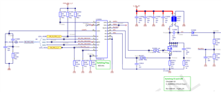
2. I've check the datasheet and the document sluaac4.pdf

My concern is about when we need to set the EN register value and when be need to read the FLT1, FLT2 register?

It's a bit confuse with me. I'm not really sure about what are actions of initializations step. Can you give me the details information and order of those actions?

What is initializations the datasheet mentioned?

Which order is correct?

Read FLT -> Set EN bit -> Write to registers to config 

OR

Set EN bit -> Write to registers to config -> Read FLT

OR

Read FLT -> Write to registers to config -> Set EN bit

Are there any delay need in each action?

3. SPI read/write issues

To write the config value to the resisters, I created a driver under Linux to do that.

But it seems that the SPI communication has some issue and I still cannot write or read the registers. I'm not sure it's my software issue or about hardware configuration issue.

I follow the instructions here to perform some write/read actions to verify the SPI communicate: tps92682-q1-what-would-be-the-response-frame-in-case-of-write-frame-following-read-frame

For example:

This is the expectation of first frame follow about ticket:
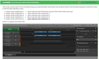
With mine, I can see that I have the same command packet on MOSI line, but the value of MISO seems not correct.

Write 0x00 to register 0x00 after POR
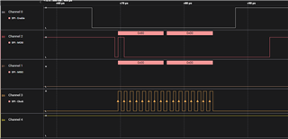
Write 1 to register 0x00
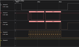
Write 2 to register 0x00
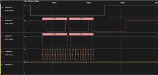
Read register 0x00
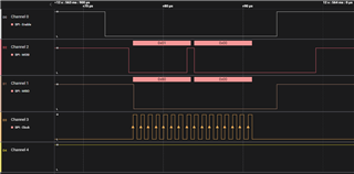
Write 3 to register 0x00
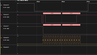
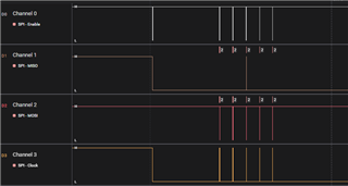
And these are all the view of 5 frames
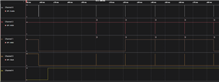
Note: The Channel 4 is the EN pin of the TPS92682

Could you please have take a look on this to see if there are anything wrong? Can it be the hardware configuration issue because I can see that the frame value seems correct?

Best regards,

Loc.

  • Hi Loc, 

    Our experts in China are on holiday this week.  Please expect delay in response.

    Best regards,

    Dave

  • Loc,

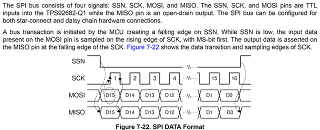
    I replied to one of your post a while back with a comment that the rising edge of the SCLK is used to sample the data.  On your system SCK is not this way...When it's rising the data on MOSI is changing.  The data needs to be stable when SCK is rising.  You need to correct this first to communicate with the part first.  

    3.  You need to read FLLT1 and FLT2 registers first then set the FPINRST to 1 in the EN register to clear the fault pins.  After that you configure all the registers and at the end you enable the part with writing a one to CHx_EN-BIT.  Note that CHx_IADJ has to have a value greater than 8 in order for the part to be enabled.  The CHx_IADJ is part of your configuration for the part.  

    On the write to  CFG1:  You should write 0x03 not 13.  LH is a Limp Home mode you need to read that section to understand more about LH and it's usage.

    You do not need to write to any of the PWM registers since you are using external PWM where the PWM1 and PWM2 pins are pulled high.  This is for constant ourput voltage.

    I would leave SoftStart register at 77 (the default value) for now.

    I would leave FEN1 and FEN2 at it's default values and not write anything to it for now.

    Again, I highly recommend you getting an evaluation board and get yourself familiarize with the part as part of you development effort.

    Thanks Tuan

  • Hi,

    Thank you very much for your information.

    But can you help clarify this:

    On your system SCK is not this way...When it's rising the data on MOSI is changing.  The data needs to be stable when SCK is rising.  You need to correct this first to communicate with the part first.

    So how can I correct this? Can you give me some suggestions? it's about my software or my hardware configuration?

    You need to read FLLT1 and FLT2 registers first then set the FPINRST to 1 in the EN register to clear the fault pins

    Then my sequence should be:

    Read FLT -> FPINRST to 1 in the EN register -> configure all the registers ->  CHx_EN-BIT set to 1 on EN register

    So there are 2 times I need to write to EN register (0x00)?

    Then may I ask, for example I want to enable 2 channel. On the 1st write to EN register the value will be 0x80 and on the 2nd write to EN register the value will be 0x83?

    Again, I highly recommend you getting an evaluation board and get yourself familiarize with the part as part of you development effort.

    Yes, sure. I really want to do that but final decision is my customer :) ... So I'm trying first to clear all the thing at my side first while waiting

    Honestly, still need your help a lot :) 


    Thank you,

    Loc.

  • Loc,

    1.  Your SCK is 180 degrees out of phase with what it needs to be.  You need to correct this in where you generate the SCK signal.  If you generate this in software, then you need to correct it there if it's hardware then you need to correct it there.

    2.  Your sequence should be as below and in flow diagram 7-20 and 7-21.  You need to read of FLT1 then a read of FLT2 then write to EN (0xBCh) then do all the writes to set up all the registers like setting it to CV mode then the ISLOPE and AIDJ ect.  After the registers are all set up then you do a write to EN to a 33 to enable the output to CH1 and CH2.  Note you are writing 33 and not 3F because you do not need  CHxPDRV to be enable in CV mode.

    3.  Part of the development is to be able to understand how the part works.  Again, you need to get the evaluation board.  There is only so much we can do over email or E2E.

    Thanks Tuan

  • Hi,

    Thank you very much for your information.

    I'm thinking that the SPI communicate still not correct.

    I want first to confirm that the software side is ok. So Could you please help do some check here:

    I'm implementing a Linux Driver to control an TPS92682.

    As from the spec, I understand that it's using the SPI Mode 0. Could you please check it?

    And here is my API that using the spi_write/spi_read to wirte/read via SPI:

    Could you please help take a look to see if my implementation is ok?

    static ssize_t tps92682_transfer(struct spi_device *spi, u16 isWrite, u16 address, u8 data)
    {
    	u16 spi92682cmd = 0;
    	ssize_t	status;
    	struct spidev_data	*spidev = spi_get_drvdata(spi);
    	int ret = 0;
    
    	mutex_lock(&spidev->buf_lock);
    
    	// AssembleSPI command
    	spi92682cmd = assembleSPICmd_682(isWrite, address, data);
    	
    	memset(spidev->tx_buffer, 0, bufsiz);
    	memset(spidev->rx_buffer, 0, bufsiz);
    	memcpy(spidev->tx_buffer, &spi92682cmd, sizeof(spi92682cmd));
    
    	if(isWrite)
    	{
    		ret = spi_write(spi,spidev->tx_buffer,2);
    		if (ret) {
    			printk("Failed writing: %d\n", ret);
    		}
    	}else
    	{
    		ret = spi_read(spi,spidev->rx_buffer,2);
    		if (ret) {
    			printk("Failed reading: %d\n", ret);
    		}
    	}
    	printk("Write/Read OK: %d\n", ret);
    	mutex_unlock(&spidev->buf_lock);
    	return status;
    }

    Here is my capture with this implement:

    Now I see that that SCK is OK now. Could you confirm it?

    Beside that, do you see any suspect point in this capture? I just concerns about the MISO line:

    1. It should be active high, is it correct?

    2. I see there are some abnormal pulse on the MISO line and the MISO keep return 0x00 all the time. Do you have any idea about this?

    3. In case that the MISO line not work, when I do the write action, do it still able to write to the TPS92682?

    Thank you.

    Best regards,

    Loc.

  • Loc,

    Your SCK is correct for MOSI but not MISO.  Again, the rising SCK needs to be when MISO data is stable.  You need to correct that in order to communicate with the TPS92682.  Again, I highly recommend you get an evaluation board and that's all we can do here.

    Thanks Tuan

  • Hi,

    Thank you.

    I just inform my customer to get one evaluation board :) . Let's wait their confirmation.

    About the current situation here.

    May I ask some questions.

    1. About the MISO line, it's keep the value 0x00 all the time? I think is abnormal, isn't it?

    2. The MISO line I see in the example is keep active high but mine is low, is it mandatory? Can I configure it via software at Linux side?

    3. Are there any method that I can check the the TPS92682 is working via some kind of measurement? If the SPI communicate of MOSI is OK. I think I already write some of the value to the TPS92682. I just want to confirm it's working or not with current hardware setup.

    Thank you very much.

  • Loc,

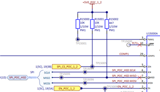
    Is there a 10K pull up register on MISO?  You need a 10K pull up to VDD of the Micro.

    The best way for you to see if you're communicating with is first to do a read of register 00h to see if it returns a default value of 3C.  If it reads 3C then do a write to register 00h for 30 and then do another read to see if it set the register to 30.  This is part of debugging your hardware to see if it's communicating.

    Thanks Tuan

  • Hi,

    I already have a pullup resistor here, could you check it?

    But I found that the MISO line is always at low level and I think that maybe the IC still not working so even the MOSI have correct data but there is no value return.

    Do you have any idea that check the device is ready? I think maybe I've do something wrong in the hardware setup and the IC still not fully power up and operation normally.

  • Loc,

    MISO is stuck LO so you will need to trouble shoot your hardware to provide appropriate communication the TPS92682. we've provided all the information for you and you will need to trouble shoot the hardware as to why it's not working.

    Thanks Tuan

  • Hi,

    Thank you very much for you support all the time here.

    I just review the HW config and found that there are another slave on the SPI bus cause the MISO line get stuck. Just update this point and the TPS92682 work find now.

    Thanks.

  • Loc,

    Glad to hear that you have resolved the issue.

    Thanks Tuan