This thread has been locked.

If you have a related question, please click the "Ask a related question" button in the top right corner. The newly created question will be automatically linked to this question.

LM7481-Q1: Reverse current protection issue

Part Number: LM7481-Q1

I've previously brought this question up in a different thread regarding the LM74801, and use of the LM74810 was recommended by Praveen as a solution because of the linear comparator's ability to block reverse current. See this thread for reference:

LM7480-Q1: LM74801-Q1: Reverse current protection issue - Power management forum - Power management - TI E2E support forums

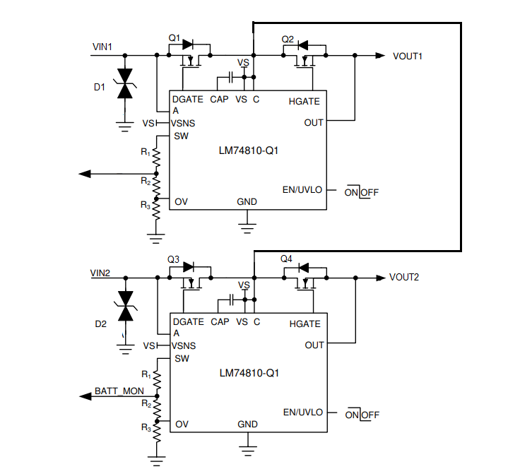
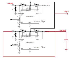
I have since respun my board, this time with the LM74810 instead of the LM74801. My circuit is for a cap bank charger that uses one 74810 to control the charge current, and one to control the output, and they are ORed together similar figure 8.6 on page 17 of the datasheet with the exception that the upper controller has both FETs and they're ORed at the common drain point. Please reference the figure below as a representation of my circuit since I am not permitted to attach a schematic:

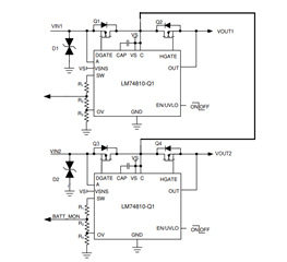
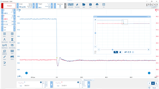
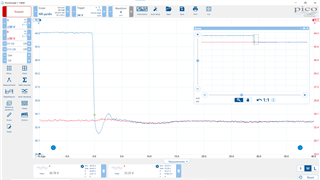
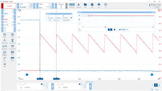
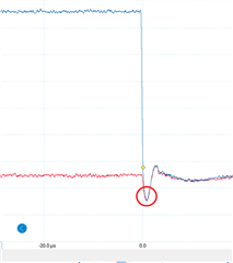
I use the upper controller to switch the charge current on and off, and VOUT1 current is monitored, as well as the voltage. When the charge voltage required is reached, a microcontroller shuts off the HGATE of the upper controller. The probelm I have with this is that the current flowing backwards through Q3 should be sufficient to shut it off. RDSon for Q3 is 1.5mR, and when the system is running, it is most likely that current is also flowing out of Q2 and backwards through Q3 simultaneously, but Q3 is not turning off. I've had everything from 0.1A to 5A flowing backward through Q3. Should this be turning off or is there something about the linear amplifier circuit that I missed that prevents it from turning off?  This poses a significant problem, and if the recommendation from Praveen to use this part was incorrect, I need to know ASAP so I can remove this part and find a different solution. 

  • Hi Jedi,

    What is the voltage measured at Vin1, Vin2, DGATE1 and DGATE2 ? Please share waveform capture with these signals captured.

    Is the 5A reverse current measured flowing through Q2, a DC current or a peak current ? Can you share waveform capture of the current as well ?

  • Please note that in this image, I've relabeled the transistors as Q1-Q4 with Q1 and Q2 being at the charger controller, and Q3 and Q4 being at the cap bank controller. Vin1 is at 38V, Vin2 is 35V, DGATE 1 and DGATE 2 are 51.5V when Vin1 is high (charger on) and DGATE 3 is at 48.5V. I can't do a waveform capture, my scope just went out for calibration (I'm remote) but I'll see if I can get my partner's scope this coming week. but the DGATE active voltage is as predicted in the datasheet.  

  • Hi Jedi,

    When you mentioned 'DGATE2', did you mean 'HGATE2' ?

    Please measure the voltages at the input/ A pin and output/C pin  of each IC.

    Also, when you capture waveforms, please capture them the signals A1, A2, C1, C2, DGATE1 and DGATE2

  • I will have my scope returned to me in 3 days and will send you the waveforms. In the interim, is my circuit diagram correct for what I'm trying to accomplish? Should DGATE2 be off when ANY current is flowing backward through Q3?

    My biggest concern is this: the unit needs to be left unsupervised, and when the processor detects that the ultra-caps are charged, it will drive EN1 low to turn off charge power to the caps. This portion of my design has been tested and works. However, as long as the charger voltage is present, the system stays alive and drains energy from the cap bank (which is its power source). My requirement is to use the charger voltage/current to keep the system alive after the charge cycle is complete. I'm charging at anywhere from 1A to 10A, depending on external criteria. My monitoring and control circuit draws 0.13A total to keep alive.

    When testing the above circuit, I charged my cap bank at 1A using a test power supply. When I drive EN1 low, HGATE1 turned off cutting off the charge current (RSENSE registers 0A), but I was still registering 1A flow from the supply. DGATE 2 was registering  about 13.1V above VIN2, telling me that Q3 was still on and was seeing reverse current. If I cut the ideal diode link (I used a wire temporarily) then the current flow drops to 0. What I am expecting to see when the charge voltage terminates is 0.13A approximately on the test power supply.  

    I've read through section 6.1 of the "Basics of Ideal Diodes" app note you suggested in my previous post, where it appears that there is no particular reference to the 748x0 family, and really doesn't' seem to offer the information I'm looking for until section 8, which apparently echos the 748x0 datasheet, and section 9 which presents a similar situation to mine (battery protection) but instead uses a PMOS incorporated device that won't work with the current levels I operate at. 

  • Hi Jedi,

    I will have my scope returned to me in 3 days and will send you the waveforms. In the interim, is my circuit diagram correct for what I'm trying to accomplish? Should DGATE2 be off when ANY current is flowing backward through Q3?

    Yes, the DGATE should be OFF (V(DGATE-A) = 0V) when the C pin voltage is greater than A pin voltage by V(AC_REV) threshold.

    If the C pin voltage is greater than A pin voltage but the difference between C and A is less than V(AC_REV) threshold, then the DGATE will be pulled low slowly by the linear gate control of LM74810-Q1.

    Regarding your circuit below,

    • The common drain point is OR'ed which means that the highest voltage of Vin1 and Vin2 will be at this node. The DGATE of the controller with the lower input voltage will be turned OFF.
    • Where is the Cap bank connected - is it connected at common drain point or Vout1 or Vout 2 ? 
    • I understand Vin1 is Charger, what is Vin2 connected to ?
    • Can you help name the nodes of your circuit in the figure below as it helps me understand your description better.

  • Hi Praveen - 

    How slowly does DGATE turn off when there's a reverse current? For instance, with a 1.5mR RDSON and a reverse current of 1A, how long should it take for DGATE to turn off? 

    Vin2 connects to the cap bank to control the power flow. Vout 2 connects to the cap bank to charge it through a sense resistor. Max current flow from the charger is 5A, minimum is ~1A, but the problem may be that when the charger is on (cc source), the voltage output drops to that of the caps, so any reverse current through Q3 should cause DGATE2 to turn off, according to section 8.3.2.1 of the datasheet that states

    "This closed loop regulation scheme enables graceful turn off of the MOSFET during a reverse current event and ensures zero DC reverse current flow." 

    So with the two power sources ORed, the charger voltage being 3V higher than the cap bank, will drop to the voltage of the cap bank if not blocked. so in my case, if there's a reverse current, the voltage is going to be really close to the cap bank voltage, but the datasheet says the linear comparator will terminate DGATE on reverse current events. Unless there's another criteria I missed in this? I'm currently re-re-reading the datasheet to determine if there's anything I missed.

    -Tony

  • Hi Tony,

    How slowly does DGATE turn off when there's a reverse current? For instance, with a 1.5mR RDSON and a reverse current of 1A, how long should it take for DGATE to turn off? 

    The linear gate control loop takes around couple of ms time to regulate the gate and pull it low to block reverse current when the reverse current magnitude is less than the [V(AC_REV)/Rds(on)] threshold. 

    • What is VOUT1 connected to ? As you have OR'ed the common drain point, how can HGATE1 help  turn ON/OFF the charge current because the cap bank is connected to the charger via Q1 and Q4 directly ?
    • I do not get the location of sense resistor in the block diagram .
    • As per your description, I have drawn the below connections. Can you help redraw the below figure with your correct system architecture if it is worng ?

    It would be easy for us to support you if you provide accurate system connection diagram. Also please waveforms as requested when available. 

  • Praveen - see attached. I've made a generic sketch of the circuit, hope it helps. The SYS OUT is power coming from the cap bank to power the system. This power is switched via Q4.

    Charge power comes into Q1, and when the charge control recognizes the power, it turns on Q2 (1 second delay). As soon as charge power comes on (before Q2 turns on), Q3 DGATE (VGS) goes to zero and stays there, as I would expect. When Q2 turns on, Q3 DGATE stays at 0V. HOWEVER - when Q2 turns off (VGS measured at 0V), Q3 DGATE starts to oscillate with a saw wave (205.4Hz) from 4V to 8V. In the interim, I'm seeing 1A from my power supply moving through Q3 (with Q2 HGATE = 0V).

  • Hi Tony,

    Thanks for the detailed explanation,

    Ideally in the two conditions - 1) Before Q2 is ON and 2) After Q2 is turned OFF (was ON previously for a while to charge the cap) the Q3 DGATE behavior should be the same as we expect the voltages at all the nodes to be the same, right ? 

    I assume the waveform shared is of Q3 DGATE in second condition above when Q2 is turned OFF. This DGATE ON/OFF behavior could be due to the following reason,

    • The Cap bank is charged close to the power supply voltage
    • The power supply voltage has significant ripple because of which there is a reverse current flow when power supply voltage > Cap bank voltage and the DGATE is turned ON when power supply voltage < Cap bank  voltage.

    Try adding more capacitance at the  input of U1 (output of power supply), the DGATE oscillations should go away.

  • Hi Praveen,

    1. At the moment of charger power input, Q3 immediately turns off because the charge voltage causes a reverse current through Q3.
    2. If I shut off and restore the charge voltage (Q2 off during this event) then Q3 will turn back on, the turn off when the charge voltage returns.
    3. If I turn on Q2:
      1. Charge voltage drops to cap bank voltage (constant current source) BUT - Q3 remains off. I presume because there is a slightly higher potential due to the ~9mv drop across Q2, making the OR point 9mV higher than Q3's source.
      2. If Q3 is off BEFORE Q2 turns on, remains off while Q2 is on, I'm not seeing the correlation with your explanation, Maybe I'm reading it wrong. 

    The power supply I use to charge the caps has only 50mV max ripple. When Q2 turns off, the charger voltage rises immediately (should be microsecond time scale) above the cap bank voltage by 3V to 4V - the ripple should have no effect on this situation because we're several volts higher. This should be sufficient to keep Q3 off. Adding bulk capacitance to the input of U1 only slows the rise by a fraction. It actually already has 20uF at the input. I will try adding more to it and testing that over the weekend.

    Could filtering Q2's gate signal help at all?

    I'll see if I can put 120uF at the input. I will update you after the weekend.

  • Hi Tony, Let me review your comments and get back to you by tomorrow.

  • Hi Praveen - any information on this issue?

  • Hi Tony,

    1. At the moment of charger power input, Q3 immediately turns off because the charge voltage causes a reverse current through Q3.
      1. In this case, is Q2 kept turned OFF ? If yes, the Q3 OFF is expected behavior 
    2. If I shut off and restore the charge voltage (Q2 off during this event) then Q3 will turn back on, the turn off when the charge voltage returns.
      1. Yes when charge input is OFF / removed, then Q3 will turn ON as there is no higher voltage connected at the Q3 drain and hence no reverse current flow. Once charge input is connected, the Q3 will turn OFF to block reverse current. This is expected behavior. 
    3. If I turn on Q2:
      1. Charge voltage drops to cap bank voltage (constant current source) BUT - Q3 remains off. I presume because there is a slightly higher potential due to the ~9mv drop across Q2, making the OR point 9mV higher than Q3's source.
        1. Yes, drop across Q2 and  Sense resistor can make the voltage at Q3 source lower than the voltage at Q3 drain causing the Q3 FET tot turn OFF. Expected behavior. 
      2. If Q3 is off BEFORE Q2 turns on, remains off while Q2 is on, I'm not seeing the correlation with your explanation, Maybe I'm reading it wrong. 
    When Q2 turns off, the charger voltage rises immediately (should be microsecond time scale) above the cap bank voltage by 3V to 4V - the ripple should have no effect on this situation because we're several volts higher. This should be sufficient to keep Q3 off.

    Your understanding is Correct. If charge voltage rises by 3V to 4V, then Q3 gate should be OFF to block reverse current. Please share waveform capture the following signals captured  at the  instant when Q2 is turned OFF - Q3 Gate, Q3 Drain, Q3 Source, Q2 Gate, 

  • Praveen, see images below. I took readings of Q3 gate, drain, and source triggered at the falling edge of Q2's gate. Gate and drain remain the same when Q2 gate drops because it's still charging, pushing the current back through Q3. The gate of Q3 oscillates at 240 Hz to 250 Hz when Q2 turns off. 

    Tony

  • Hi Tony, What are the signals in red in the first two waveforms ? Is the red signal in the first waveform Source of Q3 and red signal in the second waveform drain ?

  • Blue is Q2 drain. Image 1 Red line is the drain of Q3, image 2 red line is the source of Q3. 

  • Hi Tony,

    I think Blue should be Q2 gate - can you confirm ?

    When Q2 turns off, the charger voltage rises immediately (should be microsecond time scale) above the cap bank voltage by 3V to 4V - the ripple should have no effect on this situation because we're several volts higher. This should be sufficient to keep Q3 off.

    Based on your description above, the Q3 drain which is connected to Q2 drain should have raised by 3-4V when Q2 gate is turned OFF. But this is not seen in the wavefroms.  

    In the 1st waveform share, when the Q2 gate is turned OFF, The Q2 gate and the Q3 drain can be seen oscillating and reaching a low value which is lower than Q3 source. 

    As the Q3 drain falls lower than the Q2 source by V(AC_FWD) threshold, the gate of Q3 has been turned ON . Looks like this first turn ON of  Q3 gate allows reverse current to flow before the linear gate control kicks in and slowly reduces the gate voltage. 

    To avoid this behavior, you will have to ensure the Q3 drain does not fall lower than the Q2 source by V(AC_FWD) when Q2 gate is turned OFF. To do this you can consider slowing down the Q2 gate falling by adding a resistor in the gate path, or by adding a snubber to GND at the Q2 drain to dampen the oscillations. 

  • Thanks Praveen.

    Yes, the Blue line is the Q2 gate. 

    Currently, I do have 5.6 ohms in series with the Q2 gate. I will increase that resistance and/or add a snubber cap, then run a few tests. I'll post my findings by end of day today. 

  • Hi Tony,

    We have holiday in TI India until 24th Oct. Will be back to office on 25th Ocy. Kindly expect a delay in response.