This thread has been locked.

If you have a related question, please click the "Ask a related question" button in the top right corner. The newly created question will be automatically linked to this question.

BQ77915: Charge FET not turning on

Part Number: BQ77915

Hi Everyone

I have a design where I make use of the BQ77915 for protection and cell balancing of a 5S battery pack. My issue is that I cannot charge the battery. I believe it is because the charge FET is being disabled for some reason, since I measure 12V on the discharge pin, but 0.4V on the charge pin.

I tried to figure out if I am triggering one of the fault conditions to cause this and found something strange. I don't need the temperature protection feature, so I added a 10k resistor from the TS pin to ground as this was my interpretation of the following statement in the datasheet: "TS: Thermistor measurement input. Connect a 10-kΩ resistor to the VSS pin if the function is not used." I thought this may be the issue, so I tried to measure the voltage on the TS pin which was 0V. I then checked the VTB pin and saw that this was also 0V. I'm guessing something is wrong there but I'm not sure what.

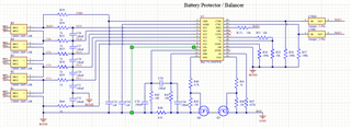
Below is my schematic. If someone can tell me if I did something wrong or give me advice to find the issue, that would be much appreciated. 

  • Hi Johannes,

    The CTRD and CTRC pins are designed to be connected to another BQ77915 device stacked above the base device, allowing BQ77915s higher in the stack to control the CHG and DSG FETs.  Currently, the way the CTRC and CTRD pins are connected may be causing issues.  Both should be connected directly to GND with no resistors.

    As far as the VTB and TS connections go: Using a 10k resistor instead of a thermistor will essentially place the device in an "always room temperature" situation since the circuit is still pulled up to VTB through a 10k resistor, and the thermistor recommended for use for the BQ77915 is 10k @ 25C. Please see the BOPM from the EVM user guide below:

    Additionally, the voltage on the VTB pin is not constant, it is a sequence of very quick pulses, so it may be hard to measure. If you want to ensure the VTB pin is functioning correctly, you can try forcing the device into a temperature fault to make sure the BQ77915 reacts appropriately.

    Best,

    Andria

  • Hi Andria

    Thank you for your thorough response. I replaced R36 and R37 with 0 ohm resistors, effectively shorting the CTRC and CTRD to BGND. Unfortunately I am still seeing the same behavior where I measure 12V on the discharge pin, but 0.4V on the charge pin, causing the FETS to disconnect BGND from GND.

    Can you think of anything else that may be causing a fault? My cells are all at 3.6V so I don't think it can be OV or UV. Please let me know what you think.

  • Hi Johannes,

    What voltage are you observing at VDD?  If VDD is < VSHUT, then the CHG driver will be inactive and prevent charging.  Please see Section 9.3.14 in the datasheet for more information. BQ77915 3-Series to 5-Series Stackable Ultra-Low Power Primary Protector with Autonomous Cell Balancing and HIBERNATE Mode datasheet (Rev. L) (ti.com)

    The Electrical Characteristics table has information on voltage threshold values:

    I also noticed that the PRES pins should be connected to VDD instead of BAT+, as showing in Figure 9-11 in the datasheet, and there should be a pulldown resistor from CBI to BGND.  I do not believe these factors should be causing the FET turn on issue, though.

    Best,

    Andria

  • Hi Andria

    Thanks for your response. I checked the VDD voltage as requested and measured it as 17.65V, so I don't think that is the issue. Do you have any other thoughts?

  • Hi Johannes,

    Although the 103 AT thermistor (recommended) should be 10kOhms at room temperature, so replacing it with a 10kOhm resistor should be okay, I would like to try replacing the resistor with a thermistor.  If this is not possible, then try pulling the TS pin to GND with a 10k resistor and leave VTB floating.

    I want to ensure that there is not a temperature fault causing CHG pin issues.

    Best,

    Andria

  • Hi Andria

    I do not have a thermistor on hand at the moment. I tried what you suggested by removing R31, leaving VTB floating. The result then was that both FETs were disabled with 0V on the DSG pin and 0.5 on the CHG pin. When I added R31 back in it was again as before with 12V on DSG and 0.4 on CHG.

    I also connected a oscilloscope to the VTB and TS pins. This was the result:

    On the VTB pin:

    On the TS pin:

    Perhaps this can help to verify that the temperature detection is working correctly?

    Please let me know if you have any other thoughts.

  • Hi Johannes,

    Yes, the waveforms show the pulsing VTB voltage, and it also looks like the device is seeing those voltages on the TS pin, just at a lower voltage level due to the resistor and thermistor resistor divider.  If you are able to get the exact voltage at the TS pin, then you can compare to the programmed OT/UT thresholds to ensure neither are triggering:

    I will continue to look over this, as your schematic doesn't seem to show major issues that I would attribute to CHG pin failing to turn on.

    Best,

    Andria

  • Hi Andria

    So the VTB pulse voltage seems to be 2.88V and the TS pulses seem to be 1.48V. That means the TS voltage is 51.4% of the VTB voltage. If I am interpreting the table correctly, that should not trigger the OT or UT thresholds. 

    This is really setting me back at the moment. If you have any other suggestions or recommendations, please let me know.

  • Hello Johannes,

    Andria is Out of Office and will be returning on Thursday, so responses may be delayed.

    I assume you've already seen Table 9-5 in the datasheet (attached for reference)

    There are a few cases where the CHG FET would be solely turned OFF. These would be OTC/UTC/OV or CTRC disabled. 

    Check every case just to make sure. Regarding the thermistor measurement, you could potentially use a power supply to forcefully apply a voltage on the TS pin and experiment different voltage ratios. The VTB pin is a 3-V pull-up. So you must make sure to keep the TS voltage below that.

    Best Regards,

    Luis Hernandez Salomon

  • Hi Luis

    I'm confident that it is not the temperature since the TS voltage does not violate any of the parameters stipulated in section 8.5 of the datasheet. and since my CTRC is pulled to ground, the only remaining option is OV. I am using the BQ7791506 so the OV threshold is 3800, yet all my cells are at 3650 mV. I will switch to the BQ7791508 next time for the higher OV threshold of 4200mV. But this should still not be a problem with the current configuration.

    Please let me know if you have any other ideas. 

  • Hi Johannes,

    Since you have confirmed that the voltage being seen at the TS pin should not cross any temperature thresholds, then I think looking at potential OV issues is a good idea due to how close the OV threshold is to your cell voltages. 

    It appears that another customer had a similar issue with measured cell voltage differing from the cell voltage the BQ77915 was seeing: (+) BQ77915: Charge mosfet continuous toggle ON - OFF - Power management forum - Power management - TI E2E support forums.  This customer was observing a toggling FET behavior instead of a constant OFF CHG FET behavior that you are seeing, but it is still good to note.

    Again, your schematic looks okay, so an unintended fault is most likely causing the CHG FET behavior.

    Best,

    Andria

  • Hi Andria

    Thanks for all your help. I am going to try to discharge the cells to see if it work when they are lower in voltage. Hopefully that works.