This thread has been locked.

If you have a related question, please click the "Ask a related question" button in the top right corner. The newly created question will be automatically linked to this question.

TPS272C45EVM: please help to check the design and analyze the reason of the high power dissipation

Part Number: TPS272C45EVM
Other Parts Discussed in Thread: LM5145, TPS272C45

Dear supplier ,

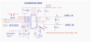
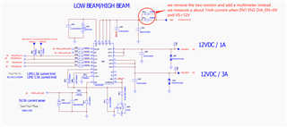
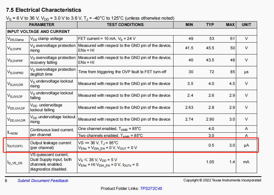
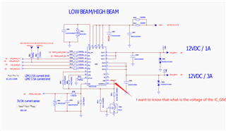
For the high side switch TPS272C45D, it may cause 0.24W power dissipation when it enters into standby mode. We measure the voltage of  the GDN pin ,there is 0.735V voltage . It is a little strange. We want to reduce the power  dissipation of the IC when into standby mode . Please review the schematic whether there is a error  and please help to analyze the reason of the high power dissipation!  Thank you very much !

  • Hello, 

    You can reduce your power dissipation by removing R815. This resistor in series with BAS21 is not needed. 

    Could you elaborate how you determined there was 0.24W of power dissipation. 

    Was this calculated or measured? Can you provide details on how this was calculated or measured? 

    Best Regards, 

    Elizabeth 

  • Dear  Elizabeth ,

    Thank you for reply !

    Change the R815 to 0R and  do the test again, the voltage of R815 is 0.644V and the power consumption has not  changed. We calculate the power dissipation is to read current change of the power supply. When we remove the R836 R833, it can cause 5mA current change  when the power supply is 48V. We also use the highside switch TPS27S100B in our design .The voltage of PIN 1 of BAS21 is almost zero when it enter into  standby mode . There is no power dissipation  problem of the TPS27S100B. Hope it can help!

    Looking forward to your reply , thank you !

  • Hello, 

    Can you clarify are you determining the power dissipation loss by seeing how much current the power supply is drawing? 

    Does this part still work after seeing this behavior or is it damaged in any way? 

    We would not expect 0.24W of power dissipation across ground when ground is measured as 0.735V. 

    Best Regards, 

    Elizabeth 

  • Dear   Elizabeth ,

    In our project, the 48V input voltage is steped down to 12V by LM5145 first ,and then supplies power to TPS272C45D. The picture below  shows the current chagne of power  supply , please check it .

    The TPS272C45D is still work after seeing this behavior.

    We test the current consumption  of TPS272C45D by multimeter when it enter into standby mode. The current is about 1mA . It is really strange, I don't know where the rest of the power goes!

    When add the R836 R833, we remove all around components of  TPS272C45D one by one , only remove R814 R815 and D803, the current of power  supply come back to 9mA.

    It seems that the stange phenomenon is appear when TPS272C45D connect to GND. Please help to analyze this problem ,thank you very much !

  • Hello, 

    Apologies for the delay. I do not see a R836 or R833 in the schematic provided. Could you please send all of the relevant parts of the schematic so I can understand what is being removed? 

    I also do not know what you are referring to when you mention only remove R814 R815 and D803 as they are not present in the provided schematic. 

    If the current is being monitored from the input of the LM5145 rather than the input of the TPS272C45D it is possible other components are contributing to the current consumption outside of the TPS272C45D. I would recommend probing the current into the TPS272C45D along with the input voltage on VS, VDD, and EN. 

    Best Regards, 

    Elizabeth 

  • Dear   Elizabeth ,

    Sorry to reply now. Please check the schematic in the attachment .5076.schematic.pdf

    We did a lot of test and finally find that the rest of the power is caused by the lm5145 itself . We use a 5K resistor instead of TPS272C45D to connect to GND and there is also a 4mA power consumption when power is 48V. It seems that  there wil be about 5mA power consumption as long as the output of the LM5145 is connected to a device which like a resistor connect to GND.

    For  TPS272C45D, when it enter into standby mode, it still consumption power (we can measure  the  ground pin is  0.735V and the current is about 1mA). How can we completely turn off the power consumption of the TPS272C45D? Is normal in standby mode when there is 0.735V voltage on GND pin?  and can we  do some actions on lm5145 to reduce the power consumption ?

    I am looking  forward to you reply ,thank you very much !

  • Fu,

    1mA is typically going to be what you see as quiescent current and is line with what we specify in the datasheet. The schematic itself looks fine and there are no issues with it.

    Best Regards,
    Tim

  • Dear Tim,

    Thank you for your reply.

    I am a little confused . The current consumption is 0.5 uA in the datasheet, please check it again? if you have any suggestions for LM5145 to redcue the standby power  consumption ? thank you very much !

  • Fu,

    I believe the confusion here is "output leakage" current versus "quiescent" current. The output leakage current is the current that leaks through from the input to the output in the OFF state while quiescent current is the current that the device consumes for operation. Were you seeing mA of current leak through from input to the output?

    Best Regards,
    Tim

  • Hi Fu, 

    To echo Tim's point, you should see uA of current from the input to the output when the device is off and ~1mA of current consumed by the device when the device is enabled. Please let us know if the device setup is in the ON or OFF state and if you are seeing mA of current leak from the input to the output. 

    Additionally with regard to your other question concerning the LM5145, unfortunately we cannot provide the best support on LM5145 as it is not part of the High-side switch portfolio. Please reach out to the BU in question by starting a new post with "LM5145" in the title for more accurate support on this part.

    Best Regards, 

    Elizabeth 

  • Dear  Tim and Elizabeth,

     Thank you for your reply. 

    We measure a about 1mA current when the device setup is OFF. please see the picture below  .Thank you all !


  • Hi Fu, 

    I do not see any issues with your schematic. What is the granularity of the ammeter being used? Can it detect uA? 

    If the VS is being shared with any other devices, that would increase the current draw. 

    The TPS272C45 device will only draw up to 3uA under the following condition when the device is off. 

    Please provide waveforms probing VS, EN, VOUT, IOUT for the relevant channel to confirm this behavior. 

    Best Regards, 

    Elizabeth 

  • Dear   Elizabeth,

    Please see the attachment. Due to the insufficient number of oscilloscope channels, I tested them separately. We did not add load, so I did not test the Iout. I really want to know what is the voltage  of IC_GND when EN and DIAG is 0V on the EVM board ?  thank you very much !

    5037.waveform.zip

  • Hello, 

    We would expect the IC_GND to have a voltage offset from module ground equal to the forward voltage drop of the diode used, which would be up to 1.25V in the case of BAS21 (shown below). 

    Do note, in your final design, the BAS21 diode specifically is not needed (another diode could be used), and in some cases we advice the BAS21 not be used. 

    To elaborate, with regard to ground network recommendations:

    On the reverse side, the diode needs to handle all the reverse standoff voltage you can see. The reason BAS21 was chosen on the EVM was to test ISO standards for the automotive version of the part. If less reverse standoff handling capability is needed, a different diode can be chosen, and another Schottky diode can be used

    The main recommendation is you don't want to see greater than 0.6V on the IC ground pin to ensure you don't unintentionally trigger the loss of ground

    Best Regards, 

    Elizabeth 

  • Dear   Elizabeth,

    Thank you for your reply .

    According to the SPEC, the max current of  IOUT(OFF) is only 3uA, but in our design ,the current is 1mA. What might be the cause of this phenomenon? thank you very much!

  • Hello, 

    Allow me to clarify the setup for the Iout(off) specification which is rated up to 3uA. 

    This specification was determined by measuring the current from the input to the output when two separate supplies are used (VDD and VS are separate sources), and VEN and VDIAG_EN are low. Under this configuration, there should only be 3uA delivered from the input to the output. This does not account for any internal circuitry powered by VDD as that would be a separate rail. 

    I am still uncertain of how you are concluding a 1mA current draw as I do not see any current measurements in the waveforms you have sent over. If you are still using the power supply to measure, it's important to consider this is also powering the LM5145 device which will be drawing current in addition to our device. Additionally if the same supply is used for VS and VDD there will be larger than 3uA of current draw from your supply. 

    My recommendation would be to measure the current directly from the VS supply into the VS pin when two independent supplies are used or the current flowing through the output when EN is low. The current measurement from the 48V supply would not be sufficient to isolate the TPS272C45's influence to the current. 

    Best Regards, 

    Elizabeth