- Ask a related questionWhat is a related question?A related question is a question created from another question. When the related question is created, it will be automatically linked to the original question.
This thread has been locked.
If you have a related question, please click the "Ask a related question" button in the top right corner. The newly created question will be automatically linked to this question.
Hello everyone,
I am currently in the process of designing a PCB with a TPS274160A (the version without the current sense capability) and I have questions regarding the GND network and and the selection of an external TVS diode.
---GND NETWORK---

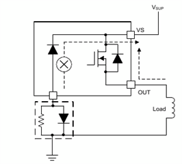
On page 24 of the datasheet, a GND network consisting of a diode in parallel with a resistor is recommended to protect the device against loss of power supply. On page 25, it is mentioned that the diode should have a current rating of >100 mA and the "forward voltage should be less than 0.6 V in any circumstances". I am having trouble determining the maximum current ("circumstances") under which the diode needs to have a voltage of <0.6V, since the mentioned >100 mA is not that precise. In the "Absolute maximum ratings", the current on the GND pin is specified to have a maximum value of -100 to 250 mA. Can I use a diode which has a voltage drop of max. 0.6V at 250 mA? For the reverse voltage rating, I suppose I have to use the maximum clamping voltage, which according to page 7 would be 70V. Is that assumption correct?
The evaluation module TPS274160EVM lists a BAS21-7-F in the BOM, but when I look at the datasheet of this diode, the forward voltage is way higher even at lower currents than the 0.6 V which is recommended. Could you please elaborate a bit more on a proper selection of the diode?
Regarding the resistor which is placed in parallel to the diode, which power dissipation should be expected? The EVM uses a .125W resistor in 0805 package, but would it be possible to use a lower power 0603 resistor?
---EXTERNAL TVS---
For additional protection against loss of power supply, I would like to add an additional TVS diode on the outputs of the device. To make sure the external TVS diode only conducts when a loss of power supply occurs, I want to increase its clamping voltage above the internal clamp of the IC. But since I still need to be below the maximum V_DS voltage the MOSFET can endure, I need this value to select a proper diode. Could you provide me this information, since I could not find it in the datasheet? Or would you recommend against an external TVS if a GND network is implemented?
Thanks in advance.
Best Regards
Hello,
---GND NETWORK---
With regard to ground network recommendations:
On the reverse side, the diode needs to handle all the reverse standoff voltage you can see. The reason BAS21 was chosen on the EVM was to test ISO standards for the automotive version of the part. If less reverse standoff handling capability is needed, a different diode can be chosen, and another Schottky diode can be used
The main recommendation is you don't want to see greater than 0.6V on the IC ground pin to ensure you don't unintentionally trigger the loss of ground
For the parallel resistance, we recommend at least a 0.125W power rating.
---EXTERNAL TVS---
For external TVS clamps, we recommend a clamping voltage below the internal TVS clamp to unintended turn-on of the FET.
The max VDS the device can handle is what the device internally clamps at.
Best Regards,
Elizabeth
Hello Elizabeth Higgins,
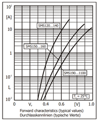
thanks for your answer. I went with a 1206 resistor for the GND network to ensure that the powerrating is definitely higher than 0.125 W. For the diode, I selected a SMS190 with a maximum reverse voltage of 90 V. This is enough for my application and the voltage drop is considerably lower than with the BAS21, but at a current of around 200 mA the typical forward voltage drop exceeds 0.6 V. But as far as I understood your post, the device will not suddenly stop working as soon as the forward voltage exceeds 0.6 V. It is more of a recommendation to be on the safe side.
For external TVS clamps, we recommend a clamping voltage below the internal TVS clamp to unintended turn-on of the FET.
The max VDS the device can handle is what the device internally clamps at.
I can see your point of choosing a TVS voltage which is lower than the internal clamp of your device, but my original idea was to choose a higher breakdown voltage on the external TVS. Under normal circumstances, the active clamp of the IC would clamp the turn-off voltage with an inductive load. The external TVS diodes would only protect the device if loss of power supply occurs, since the active clamp will not work then. This is why I asked for the exact specification of the internal FET.
Hi Marvin,
It is required for the forward voltage to not exceed 0.6V to ensure there is no unintended loss of ground which would disable the switch. Fortunately however, you do not need to look at the forward voltage of the Schottky diode you've selected at 200mA, but instead at the max quiescent current of the switch (6.2mA), shown below and in the datasheet:

This will be the max current through the ground pin of the device into the Schottky diode.
Based on the SMS190 diode you have selected, the forward voltage of the diode at 6mA will be less than 0.4V which is more than sufficient.

The internal Vds clamp ranges in voltage as shown below and in the datasheet:

Best Regards,
Elizabeth
Hi Elizabeth,
thanks for explaining further.
Fortunately however, you do not need to look at the forward voltage of the Schottky diode you've selected at 200mA, but instead at the max quiescent current of the switch (6.2mA), shown below and in the datasheet:
This was exactly the information I was looking for. I was a bit confused because in the datasheet you state "The reverse current protection diode in the GND network forward voltage should be less than 0.6 V in any circumstances", but it was unclear to me what you meant with "any circumstances". Your post cleared things up for me by specifying that the quiescent current is the value I need to keep in mind when selecting a diode. Now the selected SMS190 indeed seems to be sufficient.
Regarding the TVS diode, I instead went with your recommendation and chose TVS diodes with a lower clamp voltage than the internal clamp of the IC. This way, the stress of clamping the voltage while turning off an inductive load is moved from the IC to the external TVS diodes.
Thanks again for your support. I will now finish the board and order some prototypes for further testing.
Best Regards,
Marvin
Hi Marvin,
Happy to help! Best of luck with the rest of your design.
Please reach out if you have any further questions.
Best Regards,
Elizabeth