This thread has been locked.

If you have a related question, please click the "Ask a related question" button in the top right corner. The newly created question will be automatically linked to this question.

TL2575HV-15: failure switch ON

Part Number: TL2575HV-15

Good day, colleagues,

My customer has the following problem:

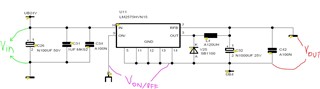
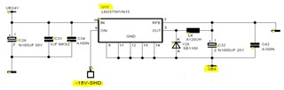
We have the Simple Step-Down Voltage Regulator type TL2575HV-151N in use on an old module.
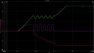
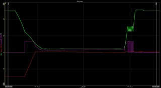
Due to failures at the customer, we have noticed that the TL2575... sporadically does not start, although the signal ON/OFF is pulled down to 0.3V by our controller. According to the data sheet, a voltage less than or equal to 0.8V should be sufficient to switch on the switching regulator safely.

The controller is operated as an inverse converter according to the following circuit diagram:

It is controlled by an optocoupler according to the following circuit diagram, since the reference ground of the ON/OFF signal is the floating -15V:

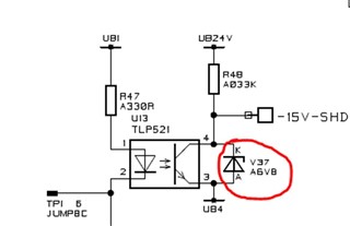
The ON/OFF signal is clamped by means of a Z-diode to 6.8V related to the generated -15V.
Can you help us understand what exactly is going on in the event of a fault? These failures are sporadic, usually starting at 60°C ambient temperature. Maximum ambient temperature is 70°C.
The connected load (at -15V) is 160 mA.
The -15V are generated from +24V.

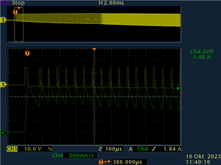
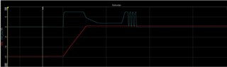
In the recording you can see the voltage at the ON/OFF pin of the switching regulator TL2575.....
The regulator was in operation: voltage at ON/OFF pin at 70 mV.
Afterwards it was switched off: Voltage at ON/OFF pin at 7.5 V.
After that it was switched on but with some jittering. But after jittering, 55 mV are permanently present.
However, the switching regulator does not switch on.

However, we make this observation very sporadically, i.e. less than one in a hundred switching regulators behaves like this.

The x-axis is scaled with 200 ms/div.

Thank you,

Daria

  • Hi Daria,

    Some startup issues can occur related to large output capacitance. It looks like there is 1mF of output capacitance on this design. Can you try reducing the value of output capacitance to 100uF and see if the behavior still occurs? Alternatively, if you have the means to measure the inductor current, you can also see if the current limit is being reached.

    When you redo this experiment, measure the SW node, Vin, Vout and ON/OFF if possible.

    Best regards,

    Ridge

  • Hi Ridge,

    For inductor current and switch node voltage see below:

    Voltage of on/off pin and output voltage is on the screenshot from initial post,

    Maybe problem is caused by on/off pin voltage jittering few times before being tied to zero by control circuit?

    Thank you,

    Daria

  • Hi Daria, 

    I am actively reviewing this issue with the team. I have a few more comments and questions:

    For the schematic, usually there is some bypass capacitance from Vin to -Vout for inverting buck boost topologies. You could try connecting C31 and C34 from Vin to -Vout.

    With regard to the Vin and ON/OFF waveform you shared earlier, I have some more questions:

    • How is the measurement taken? Since the IC is referenced to -Vout by the inverting buck boost topology, it does not make sense to me that the device should turn on when you measure 0V on the scope. 0V on the scope should be +15V on the ON/OFF pin since 0V - (-Vout) = 15. 10V on the scope would be even higher with respect to -Vout. 
    • Can you share a photo of the test setup, and can you show a waveform that includes Vout, Vin, and ON/OFF?

    Here is a link to a useful generalized app note on IBB converters: https://www.ti.com/lit/an/snva856b/snva856b.pdf

    Best regards,

    Ridge

  • Hi Ridge,

    Vin and Vout are measured to GND. On/off is measured with a differential probe to Vout.

    This is the schematic of test setup:

    See screenshot below for a normal start-up sequence of buck-boost regulator:

    (Time base is 50ms/div.)


    See screenshot below for a faulty start-up sequence of buck-boost regulator:

    (time base is 500ms/div.)

    Thank you,

    Daria

  • Hi Daria,

    Have you been able to test the design with the correct orientation of the bypass capacitor from Vin to -Vout? The "Working with Inverting Buck Boost Converters" shows examples of how the Cio capacitor needs to be configured: https://www.ti.com/lit/an/snva856b/snva856b.pdf

    You may need to smooth the ON/OFF signal. The bouncing could be causing issues. 

    Why is the power supply falling during the faulty example? That could be having an impact as well.

    Best regards,

    Ridge

  • Hello,

    Since we have not heard back in a while, I will close this thread. If you have more questions, you can re-open this thread by replying or open a new thread.

    Best regards,

    Ridge