Hi,
Below is my schematic arround TPS7A3301RGWT for my custom board, i have tried to maximum follow the EVK
But still i wish to know if there are any flaws in my layout
Kindly have a look and drop your valuabel comments
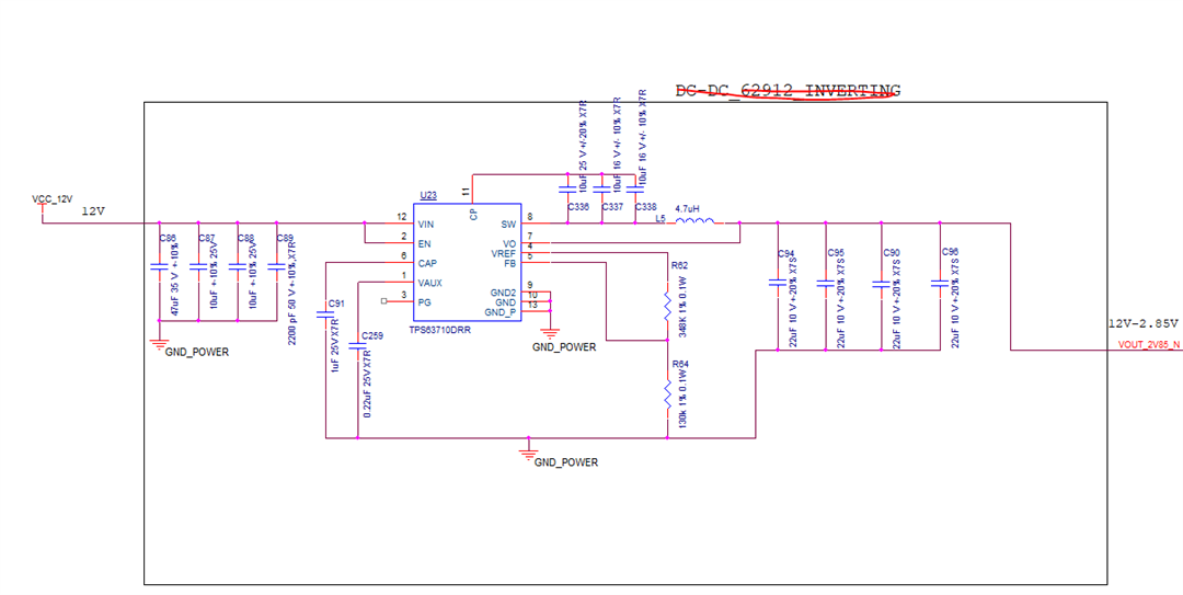
Schematic:
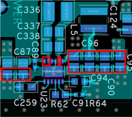
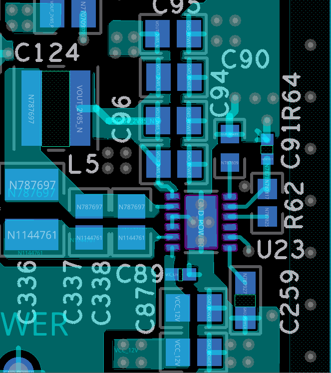
Layout:
Hi,
Below is my schematic arround TPS7A3301RGWT for my custom board, i have tried to maximum follow the EVK
But still i wish to know if there are any flaws in my layout
Kindly have a look and drop your valuabel comments
Schematic:
Layout: