This thread has been locked.

If you have a related question, please click the "Ask a related question" button in the top right corner. The newly created question will be automatically linked to this question.

TPS6521905: [TPS6521907RHB]3V3 output issue

Part Number: TPS6521905


Hi team:

 my customer using TPS6521907RHB device.

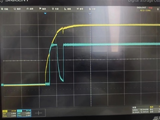
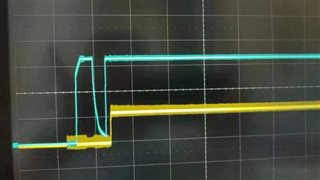
Here attach the power-on waveform of tps6521907. The yellow color is enable signal and the blue color is 3.3 vol. But I don’t know why at 3.3 volts, it is powered on first, then powered off, and then powered on again. So could you please help me find out what is going on?  tks ~
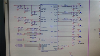
SCH:

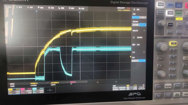
blue :3v3 ,yellow :1.2V

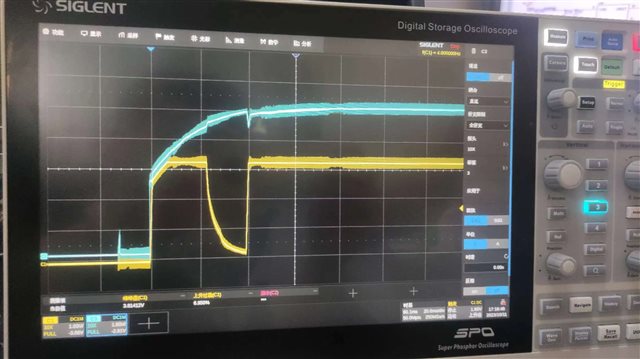
enable yellow ,blue: 3v3 vol

  • Hi,

    Thanks for reaching out. Could you please provide the schematic in a searchable PDF instead or image? We would like to review the PMIC and any pull-up or circuitry driving the digital signals. Additionally, could you provide a power-up capture (showing the oscilloscope x/y scale) of the following signals:

    • VSYS (PS5V)
    • EN/PB/VSENSE (3.3V_EN)
    • Buck2 (V3.3V)
    • LDO2 (V1.8Vv)
    • nRSTOUT (PMIC_nRST)

    Please include as many signals (channels) as possible in the same scope capture. 

    Thanks,

    Brenda

  • Hi Brenda:

     Tks for the comments. I found the reason why show as above waveform.  Customer use DIY 5V adapter for debug purpose.

     We can see the 5V VSYS ramp up time is about 60ms. when we choose to use the normal USB 5v to supply, the ramp up time is around 5ms ,then the abnormal issue all disappear.

    Yellow: 5V, blue: 3v3

    blue :enable, yellow : 3v3

    So my question IS:

    1. What are the requirements for ramp up timing of Vsys?

    2. What the different of Buck 2 and Buck 3 from Vsys?  Because the buck3 of 1.2V with abnormal 5V show no issue.

     tks for the comments.

  • Hi,

    Thanks for sharing an update and letting us know the issue is resolved when using the normal USB 5V with a faster ramp. The pre-regulator that supplies VSYS must reach a stable Vout within 2.3ms after VSYS goes above the POR threshold. See section "6 VSYS Voltage Ramp" on the AM62x Apps note for more information and let us know if you have any questions. (Here is the link for the Apps note and TRM: https://www.ti.com/lit/pdf/slvafd0).

    • Please note LDO1 does not follow our guidelines in the customer schematic. This LDO is configured as bypass and the output voltage controlled by the VSEL_SD digital pin with the following polarity:
      • SEL_SD High: LDO1=3.3V (behaves as Bypass and requires 3.3V at the input (PVIN_LDO1)
      • VSEL_SD Low: LDO1=1.8V

    • The input capacitance for Buck3 (PVIN_B3) does not meet the spec. This pin requires a typical of 4.7uF capacitance or higher.

    • VDD1P8 (internal LDO) requires 2.2uF capacitance (Typical). 

    Thanks,

    Brenda