Sometimes it can be challenging to simulate devices models in PSpice For TI given all the different buttons and knobs. The intent behind this post is to guide the reader on how to simulate the TPSI305x-Q1 models in PSpice For TI to aid the design-in process. The following assumes PSpice For TI is already installed. The Explore PSpice for TI design and simulation tool video series can be viewed here for additional guidance.
Opening TPSI305x-Q1 Model in PSpice For TI
- Download TPSI305x-Q1 PSpice Model (SLVMDV1C.ZIP) and Calculation Tool (SLVRBI9) from product page.
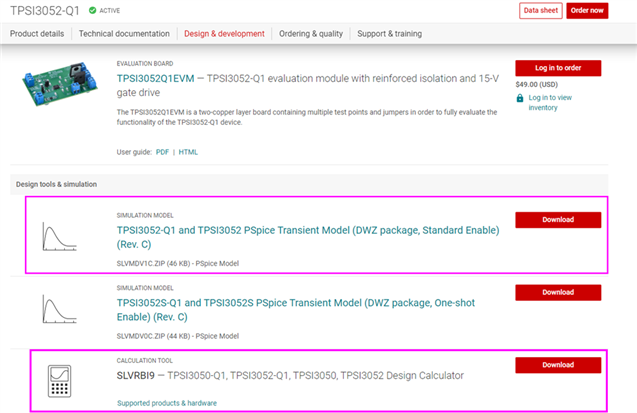
Figure 1: TPSI305x-Q1 Product Page View
- Run PSpice For TI and open TPSI305x-Q1 testbench.
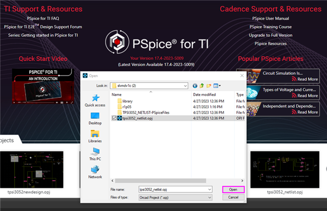
Figure 2: Opening TPSI305x-Q1 Testbench
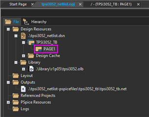
Figure 3: Opening TPSI305x-Q1 Testbench
Determining CVDRV, CDIV1, and CDIV2
Electrical concepts can often be compared to water. Using this analogy, the TPSI305x-Q1 can be likened to a water delivery system for a pool. The power transfer setting corresponds to the volume of water being delivered to the pool. Each activation (drive) of a MOSFET can be thought of as scooping out some water, leading to a drop in the pool's water level. The bigger the pool, the smaller the drop for each scoop. In this example, the pool represents the CDIV1 and CDIV2 capacitors. With every MOSFET activation, a specific charge is injected into its gate. This charge is taken from CDIV1 and CDIV2, resulting in a voltage drop (VDDHdroop and VDDMdroop). Therefore, CDIV1 and CDIV2 should be adequately sized. The amount of charge is determined by the total gate charge specification in the MOSFET datasheet and can be modelled as a capacitor, CVDRV.
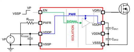
Figure 4: TPSI305x-Q1 with MOSFET Diagram
- Select MOSFET and determine total gate charge from datasheet for sizing load capacitor (CVDRV) in testbench. In this example, we use a MOSFET from the EVM.
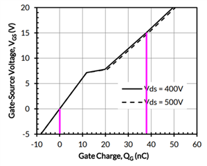
Figure 5: UJ4C075060K3S Vgs vs. Qg Graph
- Total gate charge = 38 nC
CVDRV=Q/V
CVDRV=38 nC/15 V (would use 10-V for TPSI3050-Q1)
CVDRV=2.53 nF - Determine CDIV1 and CDIV2 using Calculation Tool (SLVRBI9). The calculation tool can also be used to understand other key parameters and how they affect performance.
- When selecting a value for VDDHdroop, consider the MOSFET’s Miller plateau, an operating region where the MOSFET is conducting current but not fully enhanced and as a result dissipating the most power (read more about Miller plateau here). Limit the voltage drop to stay above the Miller plateau in addition to auxiliary circuitry receiving power from VDDM and VDDH and their absolute maximum specifications.
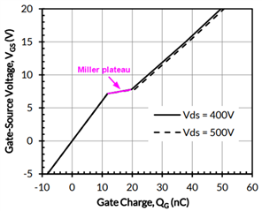

Figure 6: Taking CDIVx from Calculation Tool
- When selecting a value for VDDHdroop, consider the MOSFET’s Miller plateau, an operating region where the MOSFET is conducting current but not fully enhanced and as a result dissipating the most power (read more about Miller plateau here). Limit the voltage drop to stay above the Miller plateau in addition to auxiliary circuitry receiving power from VDDM and VDDH and their absolute maximum specifications.
- Set CDIV1, CDIV2, and CVDRV values in testbench. For the sake of realistic capacitances, CDIV1=100 nF, CDIV2=330 nF
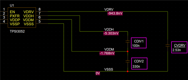
Figure 7: Setting CDIVx and CVDRV in PSpice
- Open PSpice > Edit Simulation Profile
- Enable Auto Converge
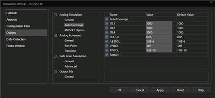
Figure 8: Enable Auto Converge
- Go to Configuration Files > Library and remove nom_pspti.lib*
- Simulating with this library file generates subcircuit errors.
Ignore, this is fixed in the PSpice model Rev. G and later updates.
- Simulating with this library file generates subcircuit errors.
- Enable Auto Converge
Simulating TPSI305x-Q1 in PSpice For TI
- Set desired switching characteristics.
- Limit switching frequency within the maximum possible switching frequency given by the calculation tool. In this case, the period should not be shorter than 10 µs.

Figure 10: Maximum Switching Frequency
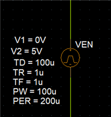
Figure 11: Setting Switching Characteristics
- Limit switching frequency within the maximum possible switching frequency given by the calculation tool. In this case, the period should not be shorter than 10 µs.
- Run simulation
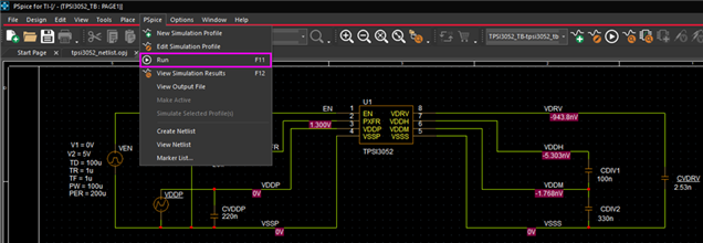
Figure 12
- View results and compare with calculation tool and datasheet. Start time, droops, and rising UVLO voltage levels seem close enough.
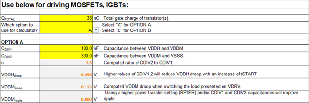
Figure 13: Calculation Tool Droop Values

Figure 14: Calculation Tool Power Transfer Table
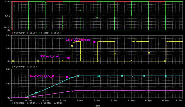
Figure 15: PSpice Results Waveforms


