This thread has been locked.

If you have a related question, please click the "Ask a related question" button in the top right corner. The newly created question will be automatically linked to this question.

TPS92519-Q1: TPS92519-Q1

Part Number: TPS92519-Q1

Hi Folks

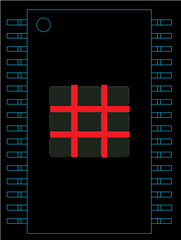
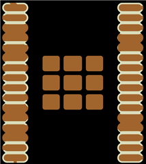
I have a question, what is better a hatching heat dissipation PAD or "square" complete PAD?

Texas Instruments always recommend a complete PAD for heat dissipation, but now we have these footprints with hatched PADs in our libraries,

but I don't know this will be affect the heat transfer to the PCB and increase the thermal resistance.

Thanks in advance.

Hector A.

  • Hello Hector,

    Based on my experience as long as the contact area is the same then the thermals will likely be very similar.  The comparative area looks almost the same.  You could measure the pad area it and verify.  

    fhoude

  • Hi Fhoude 

    Thanks for your replay.

    The area of hatched PAD is less than the physical Thermal PAD under the IC

    The lines in red the footprint don't have contact with the physical PAD in the IC, for this reason I think is better to have a completed PAD and not hatched.

    What do you think?

    Thanks

  • I agree that a non hatched pad is slightly better for thermals but when comparing thermal resistances from the junction of the device to the ambient air environment this will not likely being the area that makes the most difference in thermal resistance.  I am not sure why they want this hatched pattern. This is not common. 

    -fhoude