This thread has been locked.
If you have a related question, please click the "Ask a related question" button in the top right corner. The newly created question will be automatically linked to this question.
Hi,TI experts
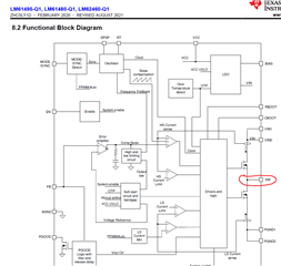
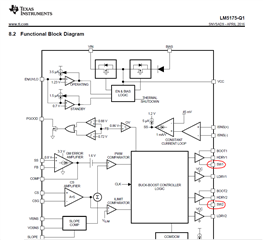
I see to LM5157 datasheet,SW1 SW2 have internal connection,I don't understand theirs function,as below image.
As I know ,Generally, Swithch node only connection Highside MOS and inductor.Could you help to me?
thank you
Hello wenjun,
For the high-side FETs, the switch node is the reference voltage for the driver signal. The gate or an NMOS needs to be higher than the source and the source of the high-side FET is the switch node.
Best regards,
Brigitte
Hello,Brigitte
Thanks for your kindly support
I am not understand clealy,could you help to explain more details.and I check LM61495 block diagram,it have no similar design,as below
thank you again
Hello wenjun,
LM5175 is a controller, so needs external MOSFETs. LM61495 is a converter with the FETs integrated. Please check the application section in the datasheet for the full schematic with external FETs.
Best regards,
Brigitte