This thread has been locked.

If you have a related question, please click the "Ask a related question" button in the top right corner. The newly created question will be automatically linked to this question.

BQ25792: BQ25792 schematic review request

Part Number: BQ25792
Other Parts Discussed in Thread: TPS25750,

Hello Sir

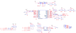
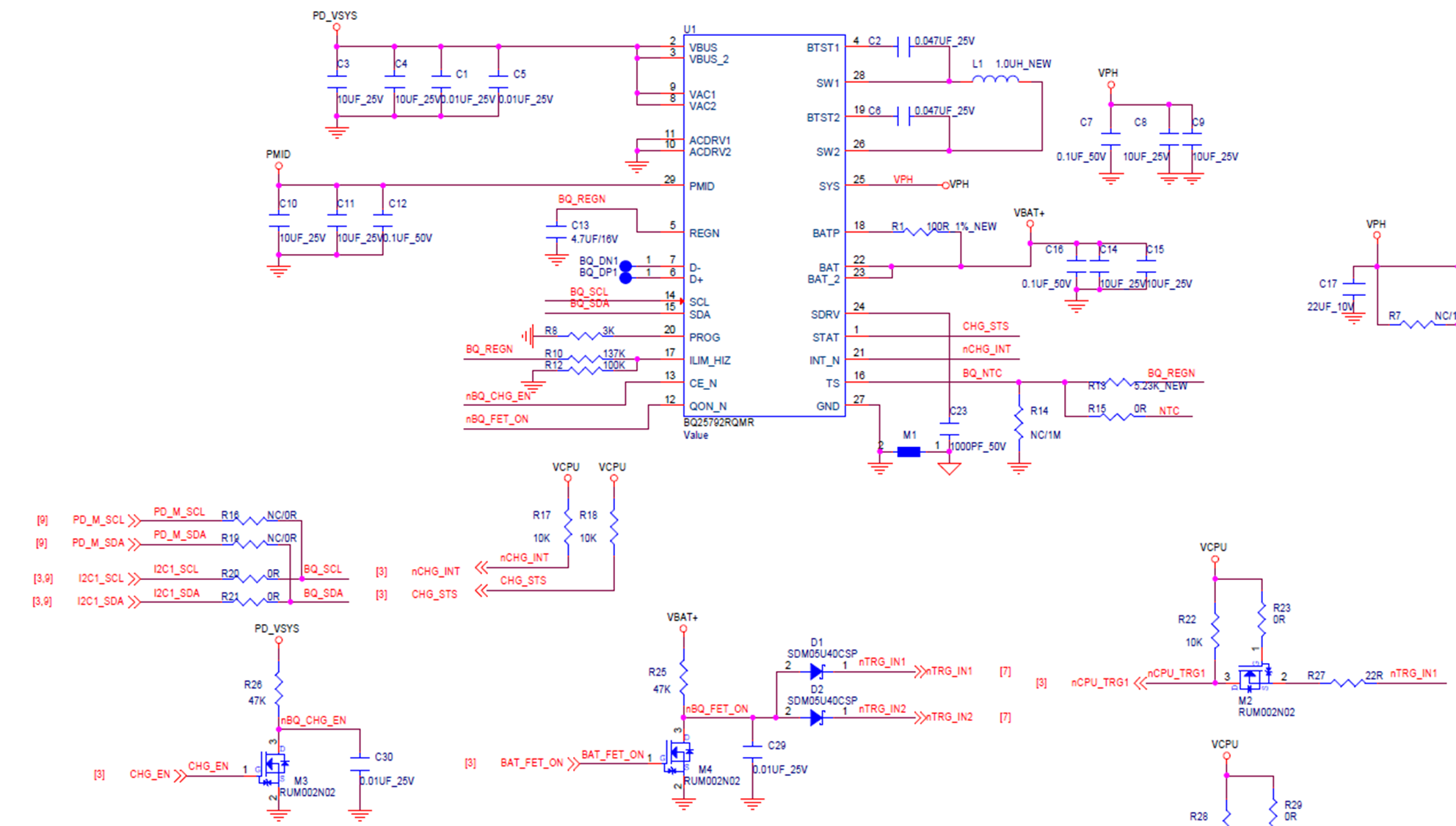
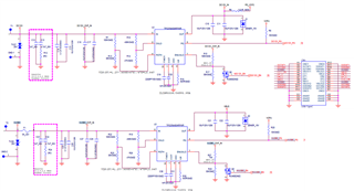
Please help us to check our schematic, we are using TPS25750+BQ25792 solutions.

We just used sink only operation on this application, is there anything I should pay attention to with the TPS25750+BQ25792 solution?

If there has any potential issues, please kindly let us know.

Looking forward your feedback.

Thanks a lot.
  • Hi Stathum,

    The charger schematic looks okay.  I will move to the PI group so they can review the TPS25750 schematic.

    Regards,

    Jeff

  • Hey Stathum,

    I'll review the TPS25750 portion and aim to give you a response by Wednesday

    Thanks and Regards,

    Chris

  • Hi Stathum,

    A couple comments and some questions.

    Schematic changes:

    • Optional
      • You can ground the PP5V pin if you are Power sink only
      • Unused GPIOs can be tied to ground. We recommend tying them to ground through 100kOhm resistors, especially if you may need them for debugging later
      • For first versions, we recommend using resistive dividers on LDO3V3 for the ADCIN pins. Unless you are 100% sure about the current configuration, using the dividers will allow for flexibility
    • Needs changes
      • Max 10uF on VBUS, you currently have 20uF
      • Recommend a 10nF capacitor on each VBUS pin of the type-c connector (CN1, 4 total)
      • CC capacitance should be 220pF with protection, or 330pF without protection
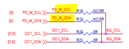
      • NC the 0 ohms connecting I2C1, and populate the PD_M_Sxx 0 ohms

    Questions:

    • What voltage is on VCPU?
    • What is the plan with U3? it looks like you are putting an additional power switch between the connector and the PD controller? Is there a reason why?
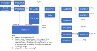
    • Could you provide a block diagram of the system?
    • What is the purpose of U2 in your system?

    Thanks and Regards,

    Chris

  • Hi Chris:

    Please refer below feedback.

    We will follow your optional and needs changes recommendations and updated schematic for you later.

    About questions.

    1. VCPU voltage is 3.3V

    2. We know that TPS25750S has no over current protections, so we put Q3 over there.

    3. According this reason we want to remove Q1 and Q2, please refer our power tree as below.

    a.We want to use the signal of gate_VBUS and gate_VSYS, when gate_VBUS or gate_VSYS signal is high, then let TPS25750S GPIO_0 or GPIO_1 output high, make an int signal for processor, then let processor to turn on TPS259460 (set nVUSBC_EN to high)

    b.Is it possible on above processing?

    4. that is the same reason with U3, we want to have OVP and OCP protections on PD_VSYS power path.

    Please let us know your feedback.

    Thanks a lot.

  • Hi Statham,

    3ab.

    Yes, you should be able to remove Q1 and Q2, and instead use just the TPS259460. 

    Is there a reason why you want to send a signal to the processor, then to the 25750s rather than just connecting them directly?

    Thanks and Regards,

    Chris

  • Hi Statham,

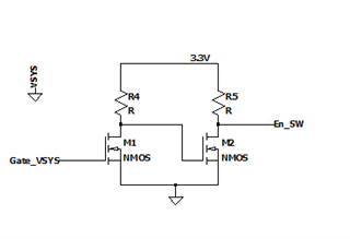
    We do not have way to implement the GPIOs as you mentioned. Instead, we recommend using a circuit similar to the one below to drive the load switch enable pin. Please note that VSYS on the TPS25750 should be grounded.

    Thanks and Regards,

    Chris