Other Parts Discussed in Thread: TL5209,
Good afternoon!
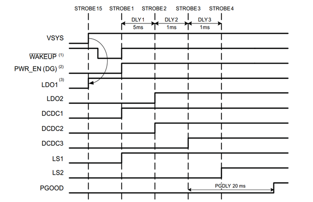
I am verifying a PCBA design with an OSD3358-512M-ICB C-SIP. This SOM contains a TPS65217C PMIC, TL5209 LDO, and an AM355x Sitara processor. It is my understanding that the power down sequence should be the reverse of the power up sequence. There are a handful of places where the power down sequence of our design does not match the reverse of the power up sequence. I would be grateful for clarification on whether we should be concerned about these variations from the expected behavior. Thanks!
Pin legend:
- PMIC_PGOOD -> TPS56217C PGOOD pin
- PMIC_LDO_PGOOD -> TPS56217C LDO_PGOOD pin
- PMIC_NWAKEUP -> TPS56217C NWAKEUP pin
- VDDSHV_3P3V -> TPS56217C LDO4
- SYS_VDD1_3P3V -> TL5209 Output
- VDD_CORE -> TPS56217C DCDC3
- VDD_MPU -> TPS56217C DCDC2
Note: I confirmed that registers 0x19 - 0x1E of the TPS56217C match the reset states for the variant of the IC.
Issues:
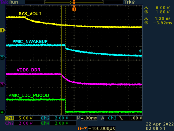
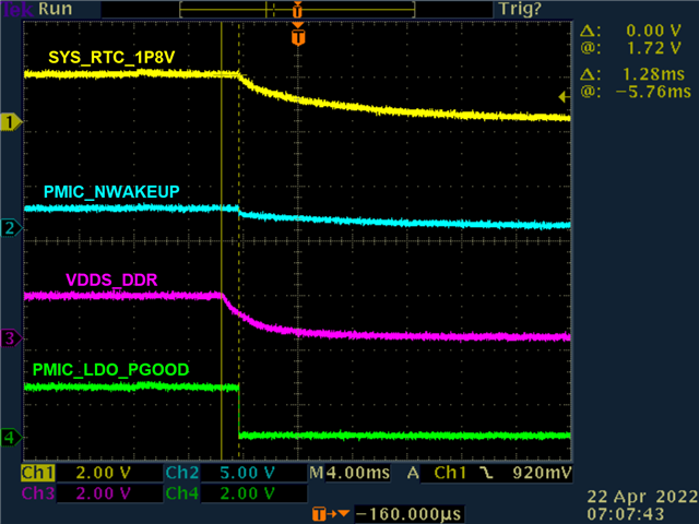
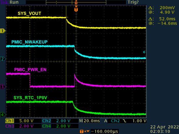
1. PMIC_PGOOD, PMIC_NWAKEUP, and PMIC_LDO_PGOOD drop-out behavior. During power-down, these three signals are briefly pulled low before decaying as expected. While not entirely clear in these first scope capture, the drop-out behavior occurs simultaneously for all three signals. In our design, these pins are all connected to pins on the AM355x processor. PMIC_PGOOD is connected to the PWRONRSTn pin, PMIC_LDO_PGOOD is connected to the RTC_PWRONRSTn pin, and PMIC_NWAKEUP is connected to the EXT_WAKEUP pin.


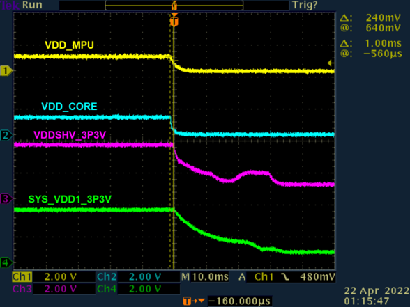
2. VDDSHV_3P3V begins to fall ~3.6 ms before VDD_CORE and VDD_MPU begin to fall. Based on the reverse power-up sequence, I would expect VDD_CORE and VDD_MPU to begin to fall about 1 ms before VDDSHV_3P3V. In our design, VDDSHV_3P3V is connected to 5/6 VDDSHV pins and to an external voltage clamping circuit.

Thank you!


