This thread has been locked.

If you have a related question, please click the "Ask a related question" button in the top right corner. The newly created question will be automatically linked to this question.

LM5026: Information regarding gate drive output section

Part Number: LM5026

Hello!

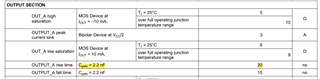
I have a question regarding the gate drive output section in LM5026 while driving MOSFET in single switch forward converter. During turn ON, the gate drive charges the gate source and gate drain capacitance of MOSFET through a gate current. However, the maximum current sourcing capability of LM5026 is not described in the datasheet. Datasheet mentions about OUTPUT_A peak current sink capability which is at 3A. What is the current source capability of the LM5026 OUTPUT A? While driving the MOSFET with higher total Qg and to reduce turn ON time, appending additional external buffer/gate drive circuit with higher current capability is recommended?

Best Regards

Samir

  • Hi Samir,

    Source current can be estimated/calculated from the Gate driver electrical characteristics from the Datasheet (see below). The rise time is 20ns. This rise time is defined as the time that takes for the driver to go from 10% to 90% Vcc (Vcc=10V according to the test conditions at the top of the table). Then delta_V=8V, Cgate=2.2nF and delta_t=20ns Then:

    I_source=Cgate*delta_V/delta_t then Isource=0.88A.

    Note: This is assuming a constant source current from the gate driver (linear increase in voltage) during the on time. Peak current is going to be a little higher than this value. 

    If you have any further questions, please let me know replyign to this thread.

  • Hi Manuel,

    Thank you for your prompt reply. The gate capacitance varies with the MOSFET we are using. The gate driver will charge the gate source and gate drain capacitance during turn ON. For a 80nC Qg MOSFET, the complete turn ON time would be (Qg/0.88A) =90 nS. So is it better to add another external gate driver for improving turn ON time with higher current capability? For turn OFF time, peak current sink capability is 3A  in datasheet, but if we follow the test condition with gate cap of 2.2nF and 15ns fall time (90% to 10%). I_sink=Cgate*del_V/del_t = 1.17A. Can you please explain the difference between these two?

    Thank you!

    Best Regards

  • Hi Samir,

    The difference comes from the fact that the gate driver capacitance Cgs is not constant. Depending on the MOSFET you are using, Cgs depends on gate to source voltage Vgs. It means that the current charging Cgs is not constant but will increase until it reaches a peak and then decrease. The calculation we used to estimate turn-on times assumed constant Cgs. The real equation should be I=dC/dt*V+C*dV/dt. 3A is the peak sink current, but not the average. The first equation gives you an idea of the average current and the turn on time, but it is not an exact number.

    if you are concerned about the on time in your MOSFET, I recommend to test LM5026 with you specific MOSFET and measure the turn on time.

    If you have any further questions, please let me know replying to this thread.

  • Hi Manuel,

    Thank you for your message. I am still confused in comprehending what you have said above. How do I quantify the drive capability of the embedded driver in LM5026. I agree turn ON time will depend on the MOSFET used, but how long do I need to turn ON any specific MOSFET depends on what is the max/average current that driver can supply? So if I know some average of max source current capability of the driver, then that can help to obtain some type of estimation of the turn ON time? please correct me if I am wrong here. I was just thinking whether there is some type of limitation that the embedded driver has and if for some application (different MOSFET) if I want to improve the drive capability, I have to go with external/additional driver.   

    I also have another question concerning the LM5026 datasheet:

    Does the CS sink impedance refer to the sinking impedance of the CS terminal when internal switch is turned ON to initiate leading edge blanking?

    Thank you so much for your support!

    Best Regards

    Samir Gautam

  • Manuel is out of the office today.

  • Hi Samir,

    Yes, the average source/sink current of the driver gives you an idea of the on/off time of the MOSFET.

    Yes, the CS sink impedance refers to the sinking impedance at the CS pin when the switch is ON.

    If you have any further questions, please let me know replying to this thread.