This thread has been locked.

If you have a related question, please click the "Ask a related question" button in the top right corner. The newly created question will be automatically linked to this question.

TPS53355: Abnormal output at low temperature –35°C

Part Number: TPS53355

Hi Team,

The TPS53355 in the circuit is used under the following conditions: VIN=12V, Vout=1.03V, Iout max =20.4A.

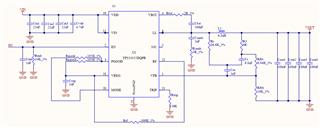
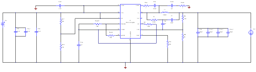
And the design is as follows:

Note:

a. All capacitors in the above figure are ceramic

b. L1 has a DCR of 1.06 mΩ

c. FSW=750kHz

Issues:

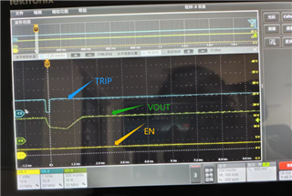
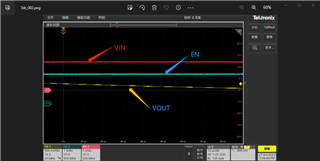
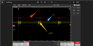
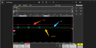
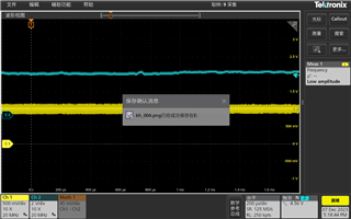
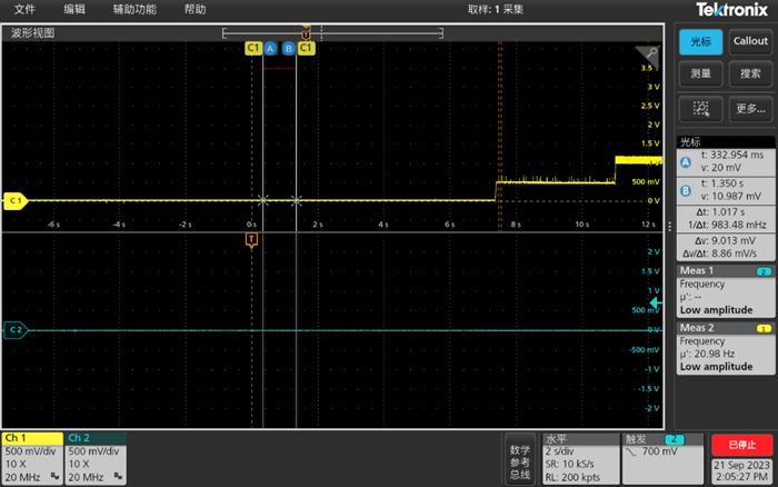
1) Some chips output about 0.5 V after power-up when at cold temperature -40°C, while it will only output the nominal voltage of 1.03 V after a few seconds. The output of the chip is good at normal temperature.

The waveform is as follows: 

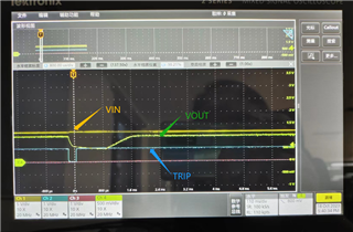
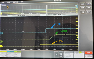
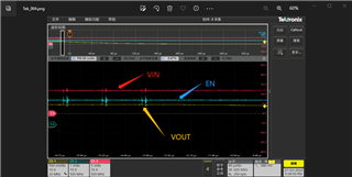
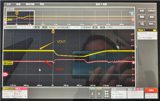
2) Some chips have dropped after a period of power-up when the temperature is -35℃. The waveform is as follows:

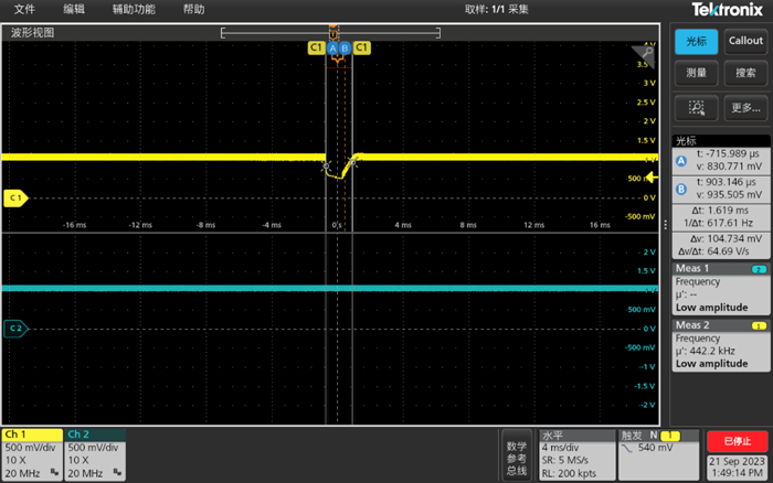
However, the chip can start up normally at low temperature -30℃. The TPS53355 output voltage is not proper, causing the system cannot start at low temperatures. 

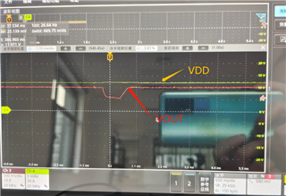
3) If the Csnub and Rsnub of the LL pin of the chip are not soldered or have wrong parameters, the chip output is only about 0.39V and cannot output the nominal voltage of 1.03V. 

And the customer has tried the following but there are no improvements:

  • Modify the Rr and Cr parameters of the ripple injection circuit to be close to L1/DCR(L1=330nH. DCR=1.06 mΩ) or decrease the DAC to 680 pF.
  • Modify the inductor value to 550nH or 160nH, other parameters are unchanged.
  • Increase capacitance, increase Cbst to 220nF, increase Cfg to 10uF, Cin adds two 22 UF capacitors and Cout adds two 100 UF capacitors.

Could you help look into the following problems:

1) What parameters does low temperature affect the TPS53355? How can these effects be reduced or eliminated?

2) Could you please help review which parameters in the circuit need to be modified?

3) What is the role of Csnub and Rsnub for the LL pin of the chip? Why does it affect output when not soldering or when parameters are not correct? 

Best Regards,

Cherry

  • Hey Cherry,

    Cold temperatures can affect current/voltage readings on any ADC/DAC within the part.

    I would request that you take oscilloscope shots of the EN, VOUT, VIN, and TRIP at startup. I would like to see if the part is maybe triggering OCP at lower temperatures. 

    Can you also provide a layout?

    Thanks,
    Caleb 

  • 1、when the chip have dropped,the waveform as follows:

    when startup ,the waveform as follows:

    2、layout file as follow

    TPS53355.brd

  • Hi Caleb,

    Thank you for the support!

    Xinjie guo is the end customer and you could continue the discussion here, please let me know if any questions.

    Best,

    Cherry

  • there is only one drop,no hiccup occurred.

  • Hey Xinjie,

    Thank you for the scope shots. Can you now put replace enable with inductor current, and make the time scale small enough so that we can see the ripple in the inductor at the time that the part shuts down.

    Also, can you give me your value of Rtrip. The schematic attached is too low resolution for me to read.

    Thanks,
    Caleb

  • Hi 

    Rtrip is 150K and the schematic as follow.

    How can I put replace enable with inductor current?What should I do?What equipment do I need to use?

    2287.TPS53355.pdf

  • Hey Xinjie,

    To measure the inductor current, you will have to unsolder one side of the inductor from the board, and then attach the lifted side back to the board using a reasonably thick wire. Then you will need to use a current probe around the wire and connect it to the oscilloscope. Like the image below.

    The reason I ask for this is I'm trying to see if the part is going into OCP by analyzing what the inductor current is doing before it shuts down.

    Thanks,
    Caleb

  • Hi

    I don't have a curent probe so I can't measure the inductor current.

    Is there any other way for me to analyze the cause of the problem?

    I measured the inductor current with a desktop multimeter, see attached video.

    When the video is interrupted, it is the position where the output drops.

    What can I do now?

  • Hey Xinjie,

    This does not help. The sampling time of the multimeter is too high. You can try varying the value of RTRIP to see the device behaves differently. I would raise the OCP value to start.

    Thanks,
    Caleb

  • Hi

    1、I increased the Rtrip to 510K, and the output still dropped at low temperatures.

    2、I reduced the Rtrip of the good power chip to 75K, and reproduced the phenomenon of low temperature output dropping.

    3、Since inductor ripple cannot be measured, are there other ideas for modification?

  • Hey Xinjie,

    Lets divert from Rtrip and take a look at your VDD voltage. I notice that you have the VDD pin connected through filtering capacitors through a via. It may be possible that the VDD voltage dropping and causing the part to go into UVLO shutdown momentarily. Can you probe the VDD voltage as close to the pin as possible?

    Thanks,
    Caleb

  • Hi

    I probe the VDD voltage on the via,and there is no dropping on the VDD voltage.The waveform as follow:

    Is there any other ideas?

    If the inductor current is increasing when VOUT dropped,what should I do?Or if the inductor current is decreasing when VOUT dropped,what should I do?

  • Hello,

    Caleb will respond to this by end of day, or tomorrow.

    Best,

    Calan

  • Hey Xinjie,

    I'm waiting on an opinion from another engineer. Thank you for your patience. 

    Best,
    Caleb

  • Hey Xinjie,

    After speaking to my colleague, we have determined that the part is not shutting down due to a fault. Which means that the part is either undergoing a UVLO shutdown and restart, or an enable toggle. 

    The next steps would be to measure EN at a smaller time scale (10us/div) to see if there is a glitch. We are focusing on EN signal since there is no filtering cap. We think there might be a small glitch that is causing the part to reset. If you can't see a glitch on Enable, I recommend disabling any bandwidth limiting you might have active. If you still can't see a glitch on enable, then check VIN with the same division settings.

    Thanks,
    Caleb

  • Hi

    I measured the EN and VIN,when Vout drops, there is no dip on EN and VIN .The waveform as follow:

    But EN and VIN have noise at the same frequency as LX.The waveform as follow:

    Could it be that VOUT is dropped by noise on EN and VIN?Or is it the noise introduced due to improper test methods?

  • Hi

    TPS53355 is enabled by another power supply.There is a capacitor of 4.7uF at the output of this power supply.

    The enable pin of the TPS53355 reserves the capacitor position, but is not soldered, on the back side of the PCB.

    How large the capacitance value needs to be?

  • Hey Xinjie,

    Yes, it looks like noise on the EN and VIN line may be causing the part to turn on and off intermittently.  Try installing a 2.2uF capacitor and report the results.

    I also notice on your schematic that enable is connected in two places. Can you confirm this?

    On the right, it looks like you may have a short that bypasses the resistor divider. Is this a schematic error?

    Thanks,
    Caleb

  • Hi

    Please refer to the attached schematic.

    4073.TPS53355.pdf

    1.I  installing a 2.2uF capacitor to enable pin,and the result is the same.The output is still abnormal at low temperatures.

    After adding the 2.2uF capacitor, the waveform of the enable pin does not improve,as follow:

    2.If it's an intermittent output anomaly caused by noise on enable and VIN, then why is the output only dropped once?

    Due to the noise originate from the LX pin, does the switching noise on the LX pin disappear then  the switching noise on the LX pin will disappear? So, the question is how to remove the noise on the LX?

    3.At low temperatures, the chip may output normally after powering on multiple times.How to explain this ?

  • Hey Xinjie,

    I will discuss this with my colleagues and get back to you soon.

    Thanks,
    Caleb

  • How's your discussion with your colleagues? Any suggestions?

  • Hey Xinjie,

    We're all pretty tied up in other things, but we have your issue on our list. My next action is to try and replicate your issue in the lab. My colleague said he'll take a look soon.

    Thanks,
    Caleb

  • Hi

    Is there any progress?

  • Hey Xinjie,

    Yes, sorry for the delay. We have come up with some other ideas as for what's going on. We noticed that on your layout, you have the VREG capacitor on the bottom layer and that there is some distance between the via and the cap. VREG also has a UVLO feature, so if the voltage drops below ~4.20V, the part will initiate a soft shut-down that will cause some of the observations you are making during your testing.

    Can you measure the voltage across the VREG cap (Creg) so that we can see if that is what is causing the UVLO?

    If that doesn't show a drop below the UVLO threshold, I would request that you place one of non-working ICs on the TPS53355 EVM and place it under the same operating conditions. My hope is that this will help us isolate the issue. If issue persists on a TI EVM, then we can move on to something wrong within the IC. If it does not follow, then we can isolate to a potential board level issue. If you need a sample, please ask Cherry.

    Thanks,
    Caleb

  • Hi

    I measured the VREG at the via ,and the waveform as follow:

    There are indeed fluctuations during power up.

    So what should I do now?Add a capacitor on the VREG?How much?

  • Hey Xinjie,

    TI recommends a minimum of 1uF on the VREG pin. I believe part of your issue is that you currently have your capacitor on the bottom layer. I would recommend you find a way to move the cap to the top layer and as close to the pin as possible. Then you can monitor VREG and VOUT like you did in the picture above.

    Thanks,
    Caleb

  • Hi

    I add a 1uF capacitor to the via on top layer of VREG,and there is no drop when TPS53355 powers up.

    I had tried to increase the cap of VREG to 10uF,but it didn't work.

    So can I say it is the position of the capacitor, not the capacitance, that affects the chip not to start. But why?What does the low temperature affect?

  • I see that this capacitor is also placed on the bottom layer on the EVM,In other words, it is not forbidden to put it on bottom layer.Thus,why my design doesn't work?

  • Hey Xinjie,

    Having filtering caps on the bottom layer introduces parasitics on the trace and via that could be magnified by the cold temperature. It is not forbidden to have the VREG cap on the bottom layer, but it definitely isn't recommended. Especially in applications with extreme operating conditions such as yours.

    Thanks,
    Caleb

  • Hi

    What do you mean by parasitics?The effect of parasitic capacitance or parasitic inductance?Or the impedance of the via?

  • Hey Xinjie,

    I'm talking about the parasitic inductance and capacitance that they VIA introduces into the signal. Mainly the parasitic inductance.

    Thanks,
    Caleb

  • Hi

    How  the parasitic inductance effect the IC?Can you elaborate on that?

  • Hey Xinjie,

    From the perspective of the VREG pin, any parasitic that does not help filter out noise is detrimental to the operation of the IC, as seen in your case.

    For your PCB, I believe the parasitic inductance is coupling on to nearby noise. The fact that your bypass circuit is NOT between the VREG pin and the VIA leads me to believe that the coupled noise is not getting filtered effectively.

    This is why I believe you need the capacitor on the top of the board, between the VREG pin and the VIA.

    Thanks,
    Caleb

  • Hi

    VREG will jitter as the load changes.The greater the load variation, the greater the fluctuation on the VREG.And I want to know why?Vreg is the output of the LDO inside the chip, so why does a load change affect it?

  • Hey Xinjie,

    The VREG may jitter due to fluctuations on the input voltage to the LDO. When a load step happens, the voltage at the input can drop momentarily, causing a drop on the VREG input voltage, this is why decoupling capacitor placement and values are important.

    I'm not sure what you are trying to show me on the oscilloscope screenshot? Is this the right photo?

    Thanks,
    Cale