This thread has been locked.

If you have a related question, please click the "Ask a related question" button in the top right corner. The newly created question will be automatically linked to this question.

LM5013-Q1: Schematic review

Part Number: LM5013-Q1

Hello,

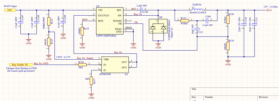
I am planning on using this device for stepping down my 30-65V battery stack to 12V with no more than 1A. Does this look ok? I have chosen a lower current rating inductor compared to WEBENCH but it is still 4A and I am only using 1A. My plan is to have a switch for the enable pin, as this goes through a voltage divider am I correct in the voltage values I have noted on the schematic?

Many thanks!

  • Hello,

    For your inductor, the part number needs to be rated for at least the peak current limit of the device which is listed 5A maximum in Section 6.5 of the datasheet. If the inductor is not properly rated, the device may not be able to protect itself during a short circuit event. 

    The coupling capacitance (C112) needs to be greater than 47pF based on your other components. With regard to the enable divider voltage values, I calculate 6.17V coming off of the divider at your max input voltage of 65V.

    This calculator is useful for determining component values: https://www.ti.com/tool/download/SNVR514

    Best regards,

    Ridge

  • Hi Ridge,

    That's great, thanks! I have changed the inductor and current value according to the design guide you sent thorugh.

    Does this look better?

    The only think is C112. The link you sent says 400pF but the datasheet says 56pF for 12V out, which one should I follow?

    Thanks!

  • Copy of LM5013 Design Calculator revB.xlsm

    Hi Mathew,

    The original value for inductance was OK with 100uH. It was the saturation current rating that needed to be addressed. You can use the 22uH if you want, but there will be more current ripple. When using this calculator, yellow boxes are values/parameters that you can adjust. I have attached an example that follows your previous design with the ripple injection network adjusted to meet my suggestion. 

    56pF for C112 will work. The calculator is not suggesting 400pF for your conditions, that it just the default value in the yellow box. When I reconfigure the calculator with your first design, the Minimum Coupling Capacitance is said to be >47pF. This means 56pF will be sufficient.

    Please let us know if you have more questions. 

    Best regards,

    Ridge

  • Hi Ridge,

    That is great, thanks again for the help! I have updated the values in accordance with that excel sheet you sent. Also, I have changed the inductor back to 100uH and at 5.3A current value (PA4344.104NLT), is this sufficient or too close to the 5A value? Only because anything other than this then the component value rises by a lot.

    Thanks!

  • Hi Matthew,

    The 5.3A rating is sufficient. One clarification about inductor ratings: your chosen inductor has a saturation current of 6.5A, which is also sufficient, according to the datasheet in the link you provided. The saturation current is the specification I have been pointing to in this thread that must be higher than the high side peak current limit. When an inductor reaches its saturation current, the value of inductance will drop significantly (manufacturer datasheets will tell you how much).

    The inductor needs to be properly rated for the whole application as you've shown with the current rating. What is important about the saturation current specification is that if the inductor saturates during a short circuit event (when current through the inductor may reach the high side current limit), the buck converter device may not be able to protect itself. 

    Your schematic looks OK. For now, I am going to close this thread. If you have more questions, you can re-open this thread by replying or you can open a new thread.

    Best regards,

    Ridge

  • Hi Ridge,

    Perfect, that makes sense now!

    Just to close it off fully please could you have a once over my layout and schematic please? I have slightly changed the enable voltage divider as the GND driven switch needs over 4.9V on it's supply pin. This should mean the device it switched off when VIN is 25V. 

    For the layout I have also minimized the loop as much as possible.

    Thanks again for the support, much appreciated!

  • Hi Matthew,

    The layout looks mostly ok. I suggest a larger ground pour around the IC as it seems like your design has the space. This will help with the thermal performance of the device. I also suggest, if possible with your ground plane, moving your input capacitors closer (C108 and C107) closer to the IC where R122 is next to C109. It is good that you have the high frequency capacitor next to the IC, but the rest of the input capacitance should be as close to the IC as possible. Here is the example layout from the datasheet for reference:

    Please note that the capacitance that is pointed out as being close to the return of the diode is for the optional RC snubber.

    Best regards,

    Ridge

  • Hi Ridge,

    Thank you, I have made the changes you suggested. Also, I have added a RC snubber, would you suggest to have this in? I could not see anything on the datasheet about it but I have used the values from a previous design I had with a TI buck-boost converter. Does this now look good?

  • Hi Matthew,

    The placement on the input capacitance looks good now. For the snubber, it is a good design practice to leave pads for the snubber if you find that you need it when you are validating the design. You do not need to populate the components unless you determine that it is necessary. The layout example from the datasheet comes from the EVM, which has pads for an optional snubber: https://www.ti.com/lit/ug/snvu754a/snvu754a.pdf

    If you look at the schematic from the EVM, you'll notice resistors and capacitors that are not populated on Vout (R3, C14, C15, C17). You do not need those pads. Those components are included on the EVM so that you could test the device using type-1 or type-2 ripple injection. Your design is using type-3 ripple injection, and looks OK.

    Best regards,

    Ridge

  • Hi Ridge,

    Understood, I will leave the snubber components as DNP for now and leave the pads included just in case I need to add once tested. I will move ahead with this design then now all looks ok. Thank you!

  • Hi Matthew,

    Glad that we could help. For now, I will close this thread. If you have more questions, you can re-open this thread by replying or create a new thread.

    Best regards,

    Ridge