Hi
The End user feedback from the Japanese market found the 1pcs battery was not charging and had no output in the system.
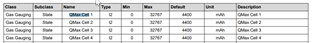
After checking the parameters, the battery has been used for 8 cycles, and the capacity data of the Qmax Cell2 became more than negative 2W, causing the battery power display to be 100 %, the battery cannot be charged or discharged.
* Texas Instruments Data Flash File
* File created Fri Oct 13 08:44:39 2023
*
* Device Number 4557
* Firmware Version 0.10
* Build Number 19
* Order Number 0
*
* bqz Device Number 4557
* bqz Firmware Version 0.10
* bqz Build Number 19
*
* Field Order: Class name	 Subclass name	 Parameter name	 Parameter Value	 Display Units
Calibration	Voltage	Cell Gain	12133	-
Calibration	Voltage	Pack Gain	49504	-
Calibration	Voltage	BAT Gain	49035	-
Calibration	Current	CC Gain	0.984	mOhm
Calibration	Current	Capacity Gain	0.984	mOhm
Calibration	Current Offset	CC Offset	0	-
Calibration	Current Offset	Coulomb Counter Offset Samples	64	-
Calibration	Current Offset	Board Offset	0	-
Calibration	Current Offset	CC Auto Config	7	hex
Calibration	Current Offset	CC Auto Offset	378	-
Calibration	Temperature	Internal Temp Offset	-2.7	degC
Calibration	Temperature	External1 Temp Offset	0	degC
Calibration	Temperature	External2 Temp Offset	0	degC
Calibration	Temperature	External3 Temp Offset	0	degC
Calibration	Temperature	External4 Temp Offset	0	degC
Calibration	Internal Temp Model	Int Gain	-12143	-
Calibration	Internal Temp Model	Int base offset	6232	-
Calibration	Internal Temp Model	Int Minimum AD	0	-
Calibration	Internal Temp Model	Int Maximum Temp	6232	0.1degK
Calibration	Cell Temperature Model	Coeff a1	-11130	-
Calibration	Cell Temperature Model	Coeff a2	19142	-
Calibration	Cell Temperature Model	Coeff a3	-19262	-
Calibration	Cell Temperature Model	Coeff a4	28203	-
Calibration	Cell Temperature Model	Coeff a5	892	-
Calibration	Cell Temperature Model	Coeff b1	328	-
Calibration	Cell Temperature Model	Coeff b2	-605	-
Calibration	Cell Temperature Model	Coeff b3	-2443	-
Calibration	Cell Temperature Model	Coeff b4	4696	-
Calibration	Cell Temperature Model	Rc0	11703	-
Calibration	Cell Temperature Model	Adc0	11703	-
Calibration	Cell Temperature Model	Rpad	0	-
Calibration	Cell Temperature Model	Rint	0	-
Calibration	Fet Temperature Model	Coeff a1	-11130	-
Calibration	Fet Temperature Model	Coeff a2	19142	-
Calibration	Fet Temperature Model	Coeff a3	-19262	-
Calibration	Fet Temperature Model	Coeff a4	28203	-
Calibration	Fet Temperature Model	Coeff a5	892	-
Calibration	Fet Temperature Model	Coeff b1	328	-
Calibration	Fet Temperature Model	Coeff b2	-605	-
Calibration	Fet Temperature Model	Coeff b3	-2443	-
Calibration	Fet Temperature Model	Coeff b4	4696	-
Calibration	Fet Temperature Model	Rc0	11703	-
Calibration	Fet Temperature Model	Adc0	11703	-
Calibration	Fet Temperature Model	Rpad	0	-
Calibration	Fet Temperature Model	Rint	0	-
Calibration	Current Deadband	Deadband	5	mA
Calibration	Current Deadband	Coulomb Counter Deadband	9	116nV
Settings	Protection	Protection Configuration	3	hex
Settings	Protection	Enabled Protections A	f7	hex
Settings	Protection	Enabled Protections B	3f	hex
Settings	Protection	Enabled Protections C	95	hex
Settings	Protection	Enabled Protections D	0f	hex
Settings	Permanent Failure	Enabled PF A	5f	hex
Settings	Permanent Failure	Enabled PF B	10	hex
Settings	Permanent Failure	Enabled PF C	73	hex
Settings	Permanent Failure	Enabled PF D	20	hex
Settings	Configuration	Charging Configuration	1	hex
Settings	Configuration	Toshiba Config	001f	hex
Settings	Configuration	Temperature Enable	14	hex
Settings	Configuration	Temperature Mode	10	hex
Settings	Configuration	DA Configuration	16	hex
Settings	Configuration	FET Options	3d	hex
Settings	Configuration	Sbs Gauging Configuration	5	hex
Settings	Configuration	Sbs Configuration	20	hex
Settings	Configuration	Power Config	0	hex
Settings	Configuration	IO Config	0	hex
Settings	Configuration	SOC Flag Config A	0c8c	hex
Settings	Configuration	SOC Flag Config B	8c	hex
Settings	Configuration	Balancing Configuration	3	hex
Settings	Configuration	IT Gauging Configuration	f3de	hex
Settings	Configuration	IT Gauging 2 Configuration	3c	-
Settings	AFE	AFE Protection Control	70	hex
Settings	AFE	ZVCHG Exit Threshold	2200	mV
Settings	Fuse	PF Fuse A	52	hex
Settings	Fuse	PF Fuse B	10	hex
Settings	Fuse	PF Fuse C	43	hex
Settings	Fuse	PF Fuse D	0	hex
Settings	Fuse	Min Blow Fuse Voltage	9000	mV
Settings	Fuse	Fuse Blow Timeout	30	s
Settings	BTP	Init Discharge Set	150	mAH
Settings	BTP	Init Charge Set	175	mAH
Settings	Manufacturing	Mfg Status init	01f8	hex
Protections	CUV	Threshold	2900	mV
Protections	CUV	Delay	2	s
Protections	CUV	Recovery	3100	mV
Protections	CUVC	Threshold	2900	mV
Protections	CUVC	Delay	2	s
Protections	CUVC	Recovery	3100	mV
Protections	COV	Threshold Low Temp	4450	mV
Protections	COV	Threshold Standard Low Temp	4450	mV
Protections	COV	Threshold Standard High Temp	4450	mV
Protections	COV	Threshold High Temp	4450	mV
Protections	COV	Threshold Rec Temp	4450	mV
Protections	COV	Delay	2	s
Protections	COV	Recovery Low Temp	4300	mV
Protections	COV	Recovery Standard Low Temp	4300	mV
Protections	COV	Recovery Standard High Temp	4300	mV
Protections	COV	Recovery High Temp	4300	mV
Protections	COV	Recovery Rec Temp	4300	mV
Protections	OCC1	Threshold	4200	mA
Protections	OCC1	Delay	1	s
Protections	OCC2	Threshold	4200	mA
Protections	OCC2	Delay	1	s
Protections	OCC	Recovery Threshold	-20	mA
Protections	OCC	Recovery Delay	5	s
Protections	OCD1	Threshold	-7500	mA
Protections	OCD1	Delay	10	s
Protections	OCD2	Threshold	-12000	mA
Protections	OCD2	Delay	2	s
Protections	OCD	Recovery Threshold	20	mA
Protections	OCD	Recovery Delay	5	s
Protections	AOLD	Latch Limit	0	-
Protections	AOLD	Counter Dec Delay	10	s
Protections	AOLD	Recovery	30	s
Protections	AOLD	Reset	15	s
Protections	AOLD	Threshold	66	hex
Protections	ASCC	Latch Limit	0	-
Protections	ASCC	Counter Dec Delay	10	s
Protections	ASCC	Recovery	30	s
Protections	ASCC	Reset	15	s
Protections	ASCC	Threshold	b0	hex
Protections	ASCD	Latch Limit	0	-
Protections	ASCD	Counter Dec Delay	10	s
Protections	ASCD	Recovery	30	s
Protections	ASCD	Reset	15	s
Protections	ASCD	Threshold 1	63	hex
Protections	ASCD	Threshold 2	63	hex
Protections	OTC	Threshold	56	1degC
Protections	OTC	Delay	2	s
Protections	OTC	Recovery	45	1degC
Protections	OTD	Threshold	70	1degC
Protections	OTD	Delay	2	s
Protections	OTD	Recovery	60	1degC
Protections	OTF	Threshold	90	1degC
Protections	OTF	Delay	2	s
Protections	OTF	Recovery	65	1degC
Protections	UTC	Threshold	4	1degC
Protections	UTC	Delay	2	s
Protections	UTC	Recovery	5	1degC
Protections	UTD	Threshold	-20	1degC
Protections	UTD	Delay	2	s
Protections	UTD	Recovery	-10	1degC
Protections	HWD	Delay	10	s
Protections	PTO	Charge Threshold	200	mA
Protections	PTO	Suspend Threshold	50	mA
Protections	PTO	Delay	3600	s
Protections	PTO	Reset	2	mAh
Protections	CTO	Charge Threshold	500	mA
Protections	CTO	Suspend Threshold	100	mA
Protections	CTO	Delay	54000	s
Protections	CTO	Reset	2	mAh
Protections	OC	Threshold	300	mAh
Protections	OC	Recovery	2	mAh
Protections	OC	RSOC Recovery	90	%
Protections	CHGV	Threshold	500	mV
Protections	CHGV	Delay	2	s
Protections	CHGV	Recovery	-500	mV
Protections	CHGC	Threshold	500	mA
Protections	CHGC	Delay	2	s
Protections	CHGC	Recovery Threshold	-20	mA
Protections	CHGC	Recovery Delay	5	s
Protections	PCHGC	Threshold	50	mA
Protections	PCHGC	Delay	2	s
Protections	PCHGC	Recovery Threshold	-20	mA
Protections	PCHGC	Recovery Delay	5	s
Permanent Fail	SUV	Threshold	1500	mV
Permanent Fail	SUV	Delay	2	s
Permanent Fail	SOV	Threshold	4500	mV
Permanent Fail	SOV	Delay	2	s
Permanent Fail	SOCC	Threshold	6000	mA
Permanent Fail	SOCC	Delay	1	s
Permanent Fail	SOCD	Threshold	-15000	mA
Permanent Fail	SOCD	Delay	2	s
Permanent Fail	SOT	Threshold	75	1degC
Permanent Fail	SOT	Delay	5	s
Permanent Fail	SOTF	Threshold	125	1degC
Permanent Fail	SOTF	Delay	5	s
Permanent Fail	Open Thermistor	Threshold	-50	1degC
Permanent Fail	Open Thermistor	Delay	5	s
Permanent Fail	Open Thermistor	Fet Delta	20	1degC
Permanent Fail	Open Thermistor	Cell Delta	20	1degC
Permanent Fail	QIM	Delta Threshold	15	%
Permanent Fail	QIM	Delay	2	updates
Permanent Fail	CB	Max Threshold	240	h
Permanent Fail	CB	Delta Threshold	40	h
Permanent Fail	CB	Delay	2	cycles
Permanent Fail	VIMR	Check Voltage	3800	mV
Permanent Fail	VIMR	Check Current	10	mA
Permanent Fail	VIMR	Delta Threshold	500	mV
Permanent Fail	VIMR	Delta Delay	5	s
Permanent Fail	VIMR	Duration	100	s
Permanent Fail	VIMA	Check Voltage	4300	mV
Permanent Fail	VIMA	Check Current	150	mA
Permanent Fail	VIMA	Delta Threshold	500	mV
Permanent Fail	VIMA	Delay	20	s
Permanent Fail	IMP	Delta Threshold	300	%
Permanent Fail	IMP	Max Threshold	400	%
Permanent Fail	IMP	Ra Update Counts	2	counts
Permanent Fail	CD	Threshold	690	mAh
Permanent Fail	CD	Delay	2	cycles
Permanent Fail	CFET	OFF Threshold	150	mA
Permanent Fail	CFET	OFF Delay	20	s
Permanent Fail	DFET	OFF Threshold	-150	mA
Permanent Fail	DFET	OFF Delay	20	s
Permanent Fail	FUSE	Threshold	5	mA
Permanent Fail	FUSE	Delay	5	s
Permanent Fail	AFER	Threshold	100	-
Permanent Fail	AFER	Delay Period	2	s
Permanent Fail	AFER	Compare Period	5	s
Permanent Fail	AFEC	Threshold	100	-
Permanent Fail	AFEC	Delay Period	5	s
Permanent Fail	2LVL	Delay	4	s
Permanent Fail	OPNCELL	Threshold	5000	mV
Permanent Fail	OPNCELL	Delay	5	s
Advanced Charge Algorithm	Temperature Ranges	T1 Temp	0	degC
Advanced Charge Algorithm	Temperature Ranges	T2 Temp	15	degC
Advanced Charge Algorithm	Temperature Ranges	T5 Temp	20	degC
Advanced Charge Algorithm	Temperature Ranges	T6 Temp	35	degC
Advanced Charge Algorithm	Temperature Ranges	T3 Temp	45	degC
Advanced Charge Algorithm	Temperature Ranges	T4 Temp	60	degC
Advanced Charge Algorithm	Temperature Ranges	Hysteresis Temp	1	degC
Advanced Charge Algorithm	Low Temp Charging	Voltage	4400	mV
Advanced Charge Algorithm	Low Temp Charging	Current Low	844	mA
Advanced Charge Algorithm	Low Temp Charging	Current Med	844	mA
Advanced Charge Algorithm	Low Temp Charging	Current High	844	mA
Advanced Charge Algorithm	Standard Temp Low Charging	Voltage	4400	mV
Advanced Charge Algorithm	Standard Temp Low Charging	Current Low	2110	mA
Advanced Charge Algorithm	Standard Temp Low Charging	Current Med	2110	mA
Advanced Charge Algorithm	Standard Temp Low Charging	Current High	1266	mA
Advanced Charge Algorithm	Standard Temp High Charging	Voltage	4400	mV
Advanced Charge Algorithm	Standard Temp High Charging	Current Low	3798	mA
Advanced Charge Algorithm	Standard Temp High Charging	Current Med	2110	mA
Advanced Charge Algorithm	Standard Temp High Charging	Current High	1266	mA
Advanced Charge Algorithm	High Temp Charging	Voltage	4200	mV
Advanced Charge Algorithm	High Temp Charging	Current Low	2110	mA
Advanced Charge Algorithm	High Temp Charging	Current Med	0	mA
Advanced Charge Algorithm	High Temp Charging	Current High	0	mA
Advanced Charge Algorithm	Rec Temp Charging	Voltage	4400	mV
Advanced Charge Algorithm	Rec Temp Charging	Current Low	3798	mA
Advanced Charge Algorithm	Rec Temp Charging	Current Med	2110	mA
Advanced Charge Algorithm	Rec Temp Charging	Current High	1266	mA
Advanced Charge Algorithm	Pre-Charging	Current	256	mA
Advanced Charge Algorithm	Maintenance Charging	Current	0	mA
Advanced Charge Algorithm	Voltage Range	Precharge Start Voltage	3000	mV
Advanced Charge Algorithm	Voltage Range	Charging Voltage Low	3000	mV
Advanced Charge Algorithm	Voltage Range	Charging Voltage Med	4200	mV
Advanced Charge Algorithm	Voltage Range	Charging Voltage High	4250	mV
Advanced Charge Algorithm	Voltage Range	Charging Voltage Hysteresis	0	mV
Advanced Charge Algorithm	Termination Config	Charge Term Taper Current	84	mA
Advanced Charge Algorithm	Termination Config	Charge Term Voltage	100	mV
Advanced Charge Algorithm	Charging Rate of Change	Current Rate	1	steps
Advanced Charge Algorithm	Charging Rate of Change	Voltage Rate	1	steps
Advanced Charge Algorithm	Charge Loss Compensation	CCC Current Threshold	690	mA
Advanced Charge Algorithm	Charge Loss Compensation	CCC Voltage Threshold	55	mV
Advanced Charge Algorithm	Cell Balancing Config	Bal Time/mAh Cell 1	320	s/mAh
Advanced Charge Algorithm	Cell Balancing Config	Bal Time/mAh Cell 2-4	448	s/mAh
Advanced Charge Algorithm	Cell Balancing Config	Min Start Balance Delta	3	mV
Advanced Charge Algorithm	Cell Balancing Config	Relax Balance Interval	18000	s
Advanced Charge Algorithm	Cell Balancing Config	Min Rsoc for Balancing	80	%
Toshiba	CRATE	CRATE Grid	128	mA
Toshiba	CV Control	CV Cycle 1	180	cycles
Toshiba	CV Control	CV Cycle 2	600	cycles
Toshiba	CV Control	CV Dec 1	12	mV
Toshiba	CV Control	CV Dec 1 Per Cycle Cylind	10	cycles
Toshiba	CV Control	CV Dec 1 Per Cycle Poly	20	cycles
Toshiba	CV Control	CV Dec 2 Cylind	16	mV
Toshiba	CV Control	CV Dec 2 Per Cycle Cylind	16	cycles
Toshiba	CV Control	CV Lifetime Cylind	43800	hours
Toshiba	CV Control	CV Lifetime Poly	4320	hours
Toshiba	CV Control	CV Dec 3	8	mV
Toshiba	CV Control	CV Dec 3 Per Hr	1152	hours
Toshiba	CV Control	CV Max Dec Threshold	620	mV
Toshiba	CV Control	CV Dec Eco	64	mV
Toshiba	Step Charge	Step Charge Voltage	4000	mV
Toshiba	Step Charge	Step Current	128	mA
Toshiba	Step Charge	Step Charge Delay	5	s
Toshiba	Step Charge	Step Current End	256	mA
Toshiba	Step Charge	CFET Time	5	s
Toshiba	Feedback Charge	Feedback Full Charge Voltage	4410	mV
Toshiba	Feedback Charge	Feedback Voltage Check Time	3	s
Toshiba	Feedback Charge	CC Full Charge Current	300	mA
Toshiba	Feedback Charge	CC Full Charge Check Time	30	s
Toshiba	Feedback Charge	CC Delta	128	mA
Toshiba	Feedback Charge	CC Min	256	mA
Toshiba	Feedback Charge	CC Hold Time	3	s
Toshiba	Feedback Charge	CC Low Temp	10	degC
Toshiba	Feedback Charge	CC Low Temp Current	500	mA
Toshiba	Feedback Charge	CC Low Temp Time	10	s
Toshiba	Eco Charge	Eco Full Charge Voltage	4200	mV
Toshiba	Eco Charge	Eco CHG RSOC	80	%
Toshiba	Eco Charge	Eco CHG RSOC Clr	0	%
Toshiba	Host Shutdown	DFET Off Threshold	5000	mV
Toshiba	Host Shutdown	SYS OFF Clear Threshold	-50	mA
Toshiba	Customer Data	Part Number	PS0123NA1BRS	-
Gas Gauging	Current Thresholds	Dsg Current Threshold	10	mA
Gas Gauging	Current Thresholds	Chg Current Threshold	50	mA
Gas Gauging	Current Thresholds	Quit Current	5	mA
Gas Gauging	Current Thresholds	Dsg Relax Time	1	s
Gas Gauging	Current Thresholds	Chg Relax Time	60	s
Gas Gauging	Design	Design Capacity mAh	4220	mAh
Gas Gauging	Design	Design Capacity cWh	4874	cWh
Gas Gauging	Design	Design Voltage	11550	mV
Gas Gauging	Cycle	Cycle Count Percentage	90	%
Gas Gauging	FD	Set Voltage Threshold	3000	mV
Gas Gauging	FD	Clear Voltage Threshold	3100	mV
Gas Gauging	FD	Set % RSOC Threshold	0	%
Gas Gauging	FD	Clear % RSOC Threshold	5	%
Gas Gauging	FC	Set Voltage Threshold	4400	mV
Gas Gauging	FC	Clear Voltage Threshold	4100	mV
Gas Gauging	FC	Set % RSOC Threshold	100	%
Gas Gauging	FC	Clear % RSOC Threshold	95	%
Gas Gauging	TD	Set Voltage Threshold	3000	mV
Gas Gauging	TD	Clear Voltage Threshold	3100	mV
Gas Gauging	TD	Set % RSOC Threshold	6	%
Gas Gauging	TD	Clear % RSOC Treshold	8	%
Gas Gauging	TC	Set Voltage Threshold	4200	mV
Gas Gauging	TC	Clear Voltage Threshold	4100	mV
Gas Gauging	TC	Set % RSOC Threshold	100	%
Gas Gauging	TC	Clear % RSOC Threshold	95	%
Gas Gauging	State	Cycle Count	8	-
Gas Gauging	State	Qmax Cell 1	4438	mAh
Gas Gauging	State	Qmax Cell 2	-21332	mAh
Gas Gauging	State	Qmax Cell 3	4486	mAh
Gas Gauging	State	Qmax Cell 4	4438	mAh
Gas Gauging	State	Qmax Pack	4438	mAh
Gas Gauging	State	Qmax Cycle Count	6	-
Gas Gauging	State	Update Status	0e	-
Gas Gauging	State	Cell 1 Chg Voltage at EoC	4392	mV
Gas Gauging	State	Cell 2 Chg Voltage at EoC	4399	mV
Gas Gauging	State	Cell 3 Chg Voltage at EoC	4400	mV
Gas Gauging	State	Cell 4 Chg Voltage at EoC	0	mV
Gas Gauging	State	Current at EoC	79	mA
Gas Gauging	State	Avg I Last Run	-321	mA
Gas Gauging	State	Avg P Last Run	-376	cW
Gas Gauging	State	Delta Voltage	333	mV
Gas Gauging	State	Temp k	10	degC/256mW
Gas Gauging	State	Temp a	18000	-
Gas Gauging	State	Max Avg I Last Run	-3641	mA
Gas Gauging	State	Max Avg P Last Run	-4440	cW
Gas Gauging	IT Cfg	Load Select	3	-
Gas Gauging	IT Cfg	Load Mode	1	-
Gas Gauging	IT Cfg	Design Resistance	81	mOhms
Gas Gauging	IT Cfg	User Rate-mA	0	mA
Gas Gauging	IT Cfg	User Rate-cW	0	cW
Gas Gauging	IT Cfg	Reserve Cap-mAh	0	mAh
Gas Gauging	IT Cfg	Reserve Cap-cWh	0	cWh
Gas Gauging	IT Cfg	Pack Resistance	15	mOhms
Gas Gauging	IT Cfg	System Resistance	10	mOhms
Gas Gauging	IT Cfg	Ra Filter	80	%
Gas Gauging	IT Cfg	Ra Max Delta	15	%
Gas Gauging	IT Cfg	Reference Grid	4	-
Gas Gauging	IT Cfg	Resistance Parameter Filter	65142	-
Gas Gauging	IT Cfg	Near EDV Ra Param Filter	59220	-
Gas Gauging	IT Cfg	Qmax Delta	5	%
Gas Gauging	IT Cfg	Qmax Upper Bound	130	%
Gas Gauging	IT Cfg	Term Voltage	9000	mV
Gas Gauging	IT Cfg	Term V Hold Time	0	s
Gas Gauging	IT Cfg	Term Voltage Delta	300	mV
Gas Gauging	IT Cfg	Term Min Cell V	3000	mV
Gas Gauging	IT Cfg	Voltage Consistency Delta	300	mV
Gas Gauging	IT Cfg	Fast Scale Start SOC	10	%
Gas Gauging	Smoothing	Smooth Relax Time	1000	s
Gas Gauging	Condition Flag	Max Error Limit	100	%
Gas Gauging	Max Error	Time Cycle Equivalent	24	h
Gas Gauging	Max Error	Cycle Delta	0.05	%
Gas Gauging	SoH	SoH Load Rate	5	hour Rate
Gas Gauging	Turbo Cfg	Min Turbo Power	-4140	cW
Gas Gauging	Turbo Cfg	Max C Rate	-4	C
Gas Gauging	Turbo Cfg	High Frequency Resistance	33	mOhms
Gas Gauging	Turbo Cfg	Reserve Energy %	0	%
Power	Power	Valid Update Voltage	3000	mV
Power	Shutdown	Shutdown Voltage	2800	mV
Power	Shutdown	Shutdown Time	10	s
Power	Shutdown	PF Shutdown Voltage	2500	mV
Power	Shutdown	PF Shutdown Time	10	s
Power	Shutdown	Charger Present Threshold	3000	mV
Power	Sleep	Sleep Current	10	mA
Power	Sleep	Bus Timeout	5	s
Power	Sleep	Voltage Time	5	s
Power	Sleep	Current Time	20	s
Power	Sleep	Wake Comparitor	0	hex
Power	Ship	FET Off Time	5	s
Power	Ship	Delay	10	s
Power	Ship	Auto Ship Time	60	min
Power	Power Off	Timeout	30	min
Power	Manual FET Control	MFC Delay	60	s
PF Status	Device Status Data	Safety Alert A	0	hex
PF Status	Device Status Data	Safety Status A	0	hex
PF Status	Device Status Data	Safety Alert B	0	hex
PF Status	Device Status Data	Safety Status B	0	hex
PF Status	Device Status Data	Safety Alert C	0	hex
PF Status	Device Status Data	Safety Status C	0	hex
PF Status	Device Status Data	Safety Alert D	0	hex
PF Status	Device Status Data	Safety Status D	0	hex
PF Status	Device Status Data	PF Alert A	0	hex
PF Status	Device Status Data	PF Status A	0	hex
PF Status	Device Status Data	PF Alert B	0	hex
PF Status	Device Status Data	PF Status B	0	hex
PF Status	Device Status Data	PF Alert C	0	hex
PF Status	Device Status Data	PF Status C	0	hex
PF Status	Device Status Data	PF Alert D	0	hex
PF Status	Device Status Data	PF Status D	0	hex
PF Status	Device Status Data	Fuse Flag	0	hex
PF Status	Device Status Data	Operation Status A	0	hex
PF Status	Device Status Data	Operation Status B	0	hex
PF Status	Device Status Data	Temp Range	0	hex
PF Status	Device Status Data	Charging Status A	0	hex
PF Status	Device Status Data	Charging Status B	0	hex
PF Status	Device Status Data	Gauging Status	0	hex
PF Status	Device Status Data	IT Status	0	hex
PF Status	Device Voltage Data	Cell 1 Voltage	0	mV
PF Status	Device Voltage Data	Cell 2 Voltage	0	mV
PF Status	Device Voltage Data	Cell 3 Voltage	0	mV
PF Status	Device Voltage Data	Cell 4 Voltage	0	mV
PF Status	Device Voltage Data	Battery Direct Voltage	0	mV
PF Status	Device Voltage Data	Pack Voltage	0	mV
PF Status	Device Current Data	Current	0	mA
PF Status	Device Temperature Data	Internal Temperature	-273.2	degC
PF Status	Device Temperature Data	External 1 Temperature	-273.2	degC
PF Status	Device Temperature Data	External 2 Temperature	-273.2	degC
PF Status	Device Temperature Data	External 3 Temperature	-273.2	degC
PF Status	Device Temperature Data	External 4 Temperature	-273.2	degC
PF Status	Device Gauging Data	Cell 1 Dod0	0	-
PF Status	Device Gauging Data	Cell 2 Dod0	0	-
PF Status	Device Gauging Data	Cell 3 Dod0	0	-
PF Status	Device Gauging Data	Cell 4 Dod0	0	-
PF Status	Device Gauging Data	Passed Charge	0	mAh
PF Status	AFE Regs	AFE Interrupt Status	0	hex
PF Status	AFE Regs	AFE FET Status	0	hex
PF Status	AFE Regs	AFE RXIN	0	hex
PF Status	AFE Regs	AFE Latch Status	0	hex
PF Status	AFE Regs	AFE Interrupt Enable	0	hex
PF Status	AFE Regs	AFE FET Control	0	hex
PF Status	AFE Regs	AFE RXIEN	0	hex
PF Status	AFE Regs	AFE RLOUT	0	hex
PF Status	AFE Regs	AFE RHOUT	0	hex
PF Status	AFE Regs	AFE RHINT	0	hex
PF Status	AFE Regs	AFE Cell Balance	0	hex
PF Status	AFE Regs	AFE AD/CC Control	0	hex
PF Status	AFE Regs	AFE ADC Mux	0	hex
PF Status	AFE Regs	AFE LED Output	0	hex
PF Status	AFE Regs	AFE State Control	0	hex
PF Status	AFE Regs	AFE LED/Wake Control	0	hex
PF Status	AFE Regs	AFE Protection Control	0	hex
PF Status	AFE Regs	AFE OCD	0	hex
PF Status	AFE Regs	AFE SCC	0	hex
PF Status	AFE Regs	AFE SCD1	0	hex
PF Status	AFE Regs	AFE SCD2	0	hex
System Data	Manufacturer Data	Manufacturer Info A Length	32	-
System Data	Manufacturer Data	Manufacturer Info Block A01	61	Hex
System Data	Manufacturer Data	Manufacturer Info Block A02	62	Hex
System Data	Manufacturer Data	Manufacturer Info Block A03	63	Hex
System Data	Manufacturer Data	Manufacturer Info Block A04	64	Hex
System Data	Manufacturer Data	Manufacturer Info Block A05	65	Hex
System Data	Manufacturer Data	Manufacturer Info Block A06	66	Hex
System Data	Manufacturer Data	Manufacturer Info Block A07	67	Hex
System Data	Manufacturer Data	Manufacturer Info Block A08	68	Hex
System Data	Manufacturer Data	Manufacturer Info Block A09	69	Hex
System Data	Manufacturer Data	Manufacturer Info Block A10	6a	Hex
System Data	Manufacturer Data	Manufacturer Info Block A11	6b	Hex
System Data	Manufacturer Data	Manufacturer Info Block A12	6c	Hex
System Data	Manufacturer Data	Manufacturer Info Block A13	6d	Hex
System Data	Manufacturer Data	Manufacturer Info Block A14	6e	Hex
System Data	Manufacturer Data	Manufacturer Info Block A15	6f	Hex
System Data	Manufacturer Data	Manufacturer Info Block A16	70	Hex
System Data	Manufacturer Data	Manufacturer Info Block A17	71	Hex
System Data	Manufacturer Data	Manufacturer Info Block A18	72	Hex
System Data	Manufacturer Data	Manufacturer Info Block A19	73	Hex
System Data	Manufacturer Data	Manufacturer Info Block A20	74	Hex
System Data	Manufacturer Data	Manufacturer Info Block A21	75	Hex
System Data	Manufacturer Data	Manufacturer Info Block A22	76	Hex
System Data	Manufacturer Data	Manufacturer Info Block A23	77	Hex
System Data	Manufacturer Data	Manufacturer Info Block A24	7a	Hex
System Data	Manufacturer Data	Manufacturer Info Block A25	78	Hex
System Data	Manufacturer Data	Manufacturer Info Block A26	79	Hex
System Data	Manufacturer Data	Manufacturer Info Block A27	30	Hex
System Data	Manufacturer Data	Manufacturer Info Block A28	31	Hex
System Data	Manufacturer Data	Manufacturer Info Block A29	32	Hex
System Data	Manufacturer Data	Manufacturer Info Block A30	33	Hex
System Data	Manufacturer Data	Manufacturer Info Block A31	34	Hex
System Data	Manufacturer Data	Manufacturer Info Block A32	35	Hex
System Data	Integrity	Static DF Signature	0	hex
System Data	Integrity	Static Chem DF Signature	507f	hex
System Data	Integrity	All DF Signature	0	hex
SBS Configuration	Data	Remaining AH Cap. Alarm	422	mAh
SBS Configuration	Data	Remaining WH Cap. Alarm	487	cWh
SBS Configuration	Data	Remaining Time Alarm	10	min
SBS Configuration	Data	Initial Battery Mode	81	hex
SBS Configuration	Data	Specification Information	31	hex
SBS Configuration	Data	Manufacture Date	2023/3/30	date
SBS Configuration	Data	Serial Number	1e6b	hex
SBS Configuration	Data	Manufacturer Name	GFL	-
SBS Configuration	Data	Device Name	G71C000MW110	-
SBS Configuration	Data	Device Chemistry	LION	-
Black Box	Safety Status	1st Status Status A	0	hex
Black Box	Safety Status	1st Status Status B	0	hex
Black Box	Safety Status	1st Safety Status C	0	hex
Black Box	Safety Status	1st Safety Status D	0	hex
Black Box	Safety Status	1st Time to Next Event	0	s
Black Box	Safety Status	2nd Status Status A	0	hex
Black Box	Safety Status	2nd Status Status B	0	hex
Black Box	Safety Status	2nd Safety Status C	0	hex
Black Box	Safety Status	2nd Safety Status D	0	hex
Black Box	Safety Status	2nd Time to Next Event	0	s
Black Box	Safety Status	3rd Status Status A	0	hex
Black Box	Safety Status	3rd Status Status B	0	hex
Black Box	Safety Status	3rd Safety Status C	0	hex
Black Box	Safety Status	3rd Safety Status D	0	hex
Black Box	Safety Status	3rd Time to Next Event	0	s
Black Box	PF Status	1st PF Status A	0	hex
Black Box	PF Status	1st PF Status B	0	hex
Black Box	PF Status	1st PF Status C	0	hex
Black Box	PF Status	1st PF Status D	0	hex
Black Box	PF Status	1st Time to Next Event	0	s
Black Box	PF Status	2nd PF Status A	0	hex
Black Box	PF Status	2nd PF Status B	0	hex
Black Box	PF Status	2nd PF Status C	0	hex
Black Box	PF Status	2nd PF Status D	0	hex
Black Box	PF Status	2nd Time to Next Event	0	s
Black Box	PF Status	3rd PF Status A	0	hex
Black Box	PF Status	3rd PF Status B	0	hex
Black Box	PF Status	3rd PF Status C	0	hex
Black Box	PF Status	3rd PF Status D	0	hex
Black Box	PF Status	3rd Time to Next Event	0	s
Lifetimes	Voltage	Cell 1 Max Voltage	4402	mV
Lifetimes	Voltage	Cell 2 Max Voltage	4403	mV
Lifetimes	Voltage	Cell 3 Max Voltage	4403	mV
Lifetimes	Voltage	Cell 4 Max Voltage	0	mV
Lifetimes	Voltage	Cell 1 Min Voltage	2670	mV
Lifetimes	Voltage	Cell 2 Min Voltage	2834	mV
Lifetimes	Voltage	Cell 3 Min Voltage	2954	mV
Lifetimes	Voltage	Cell 4 Min Voltage	32767	mV
Lifetimes	Voltage	Max Delta Cell Voltage	499	mV
Lifetimes	Current	Max Charge Current	3801	mA
Lifetimes	Current	Max Discharge Current	-5343	mA
Lifetimes	Current	Max Avg Dsg Current	-4623	mA
Lifetimes	Current	Max Avg Dsg Power	-4440	cW
Lifetimes	Temperature	Max Temp Cell	40	degC
Lifetimes	Temperature	Min Temp Cell	15	degC
Lifetimes	Temperature	Max Delta Cell Temp	0	degC
Lifetimes	Temperature	Max Temp Int Sensor	46	degC
Lifetimes	Temperature	Min Temp Int Sensor	14	degC
Lifetimes	Temperature	Max Temp Fet	50	degC
Lifetimes	Safety Events	No Of COV Events	0	events
Lifetimes	Safety Events	Last COV Event	0	cycles
Lifetimes	Safety Events	No Of CUV Events	6	events
Lifetimes	Safety Events	Last CUV Event	8	cycles
Lifetimes	Safety Events	No Of OCD1 Events	0	events
Lifetimes	Safety Events	Last OCD1 Event	0	cycles
Lifetimes	Safety Events	No Of OCD2 Events	0	events
Lifetimes	Safety Events	Last OCD2 Event	0	cycles
Lifetimes	Safety Events	No Of OCC1 Events	0	events
Lifetimes	Safety Events	Last OCC1 Event	0	cycles
Lifetimes	Safety Events	No Of OCC2 Events	0	events
Lifetimes	Safety Events	Last OCC2 Event	0	cycles
Lifetimes	Safety Events	No Of AOLD Events	0	events
Lifetimes	Safety Events	Last AOLD Event	0	cycles
Lifetimes	Safety Events	No Of ASCD Events	0	events
Lifetimes	Safety Events	Last ASCD Event	0	cycles
Lifetimes	Safety Events	No Of ASCC Events	0	events
Lifetimes	Safety Events	Last ASCC Event	0	cycles
Lifetimes	Safety Events	No Of OTC Events	0	events
Lifetimes	Safety Events	Last OTC Event	0	cycles
Lifetimes	Safety Events	No Of OTD Events	0	events
Lifetimes	Safety Events	Last OTD Event	0	cycles
Lifetimes	Safety Events	No Of OTF Events	0	events
Lifetimes	Safety Events	Last OTF Event	0	cycles
Lifetimes	Charging Events	No Valid Charge Term	3	events
Lifetimes	Charging Events	Last Valid Charge Term	7	cycles
Lifetimes	Gauging Events	No Of Qmax Updates	4	events
Lifetimes	Gauging Events	Last Qmax Update	6	cycles
Lifetimes	Gauging Events	No Of Ra Updates	142	events
Lifetimes	Gauging Events	Last Ra Update	8	cycles
Lifetimes	Gauging Events	No Of Ra Disable	21	events
Lifetimes	Gauging Events	Last Ra Disable	8	cycles
Lifetimes	Power Events	No Of Shutdowns	22	events
Lifetimes	Cell Balancing	Cb Time Cell 1	0	h
Lifetimes	Cell Balancing	Cb Time Cell 2	2	h
Lifetimes	Cell Balancing	Cb Time Cell 3	0	h
Lifetimes	Cell Balancing	Cb Time Cell 4	0	h
Lifetimes	Time	Total Fw Runtime	1300	h
Lifetimes	Time	Time Spent In UT	0	h
Lifetimes	Time	Time Spent In LT	2	h
Lifetimes	Time	Time Spent In STL	4	h
Lifetimes	Time	Time Spent In RT	1234	h
Lifetimes	Time	Time Spent In STH	44	h
Lifetimes	Time	Time Spent In HT	0	h
Lifetimes	Time	Time Spent In OT	0	h
Ra Table	R_a0	Cell0 R_a flag	55	-
Ra Table	R_a0	Cell0 R_a 0	49	2^-10ohm
Ra Table	R_a0	Cell0 R_a 1	85	2^-10ohm
Ra Table	R_a0	Cell0 R_a 2	88	2^-10ohm
Ra Table	R_a0	Cell0 R_a 3	97	2^-10ohm
Ra Table	R_a0	Cell0 R_a 4	100	2^-10ohm
Ra Table	R_a0	Cell0 R_a 5	112	2^-10ohm
Ra Table	R_a0	Cell0 R_a 6	121	2^-10ohm
Ra Table	R_a0	Cell0 R_a 7	112	2^-10ohm
Ra Table	R_a0	Cell0 R_a 8	105	2^-10ohm
Ra Table	R_a0	Cell0 R_a 9	116	2^-10ohm
Ra Table	R_a0	Cell0 R_a 10	153	2^-10ohm
Ra Table	R_a0	Cell0 R_a 11	149	2^-10ohm
Ra Table	R_a0	Cell0 R_a 12	206	2^-10ohm
Ra Table	R_a0	Cell0 R_a 13	462	2^-10ohm
Ra Table	R_a0	Cell0 R_a 14	6377	2^-10ohm
Ra Table	R_a1	Cell1 R_a flag	55	-
Ra Table	R_a1	Cell1 R_a 0	48	2^-10ohm
Ra Table	R_a1	Cell1 R_a 1	82	2^-10ohm
Ra Table	R_a1	Cell1 R_a 2	85	2^-10ohm
Ra Table	R_a1	Cell1 R_a 3	93	2^-10ohm
Ra Table	R_a1	Cell1 R_a 4	104	2^-10ohm
Ra Table	R_a1	Cell1 R_a 5	102	2^-10ohm
Ra Table	R_a1	Cell1 R_a 6	108	2^-10ohm
Ra Table	R_a1	Cell1 R_a 7	113	2^-10ohm
Ra Table	R_a1	Cell1 R_a 8	109	2^-10ohm
Ra Table	R_a1	Cell1 R_a 9	122	2^-10ohm
Ra Table	R_a1	Cell1 R_a 10	165	2^-10ohm
Ra Table	R_a1	Cell1 R_a 11	170	2^-10ohm
Ra Table	R_a1	Cell1 R_a 12	232	2^-10ohm
Ra Table	R_a1	Cell1 R_a 13	503	2^-10ohm
Ra Table	R_a1	Cell1 R_a 14	6990	2^-10ohm
Ra Table	R_a2	Cell2 R_a flag	55	-
Ra Table	R_a2	Cell2 R_a 0	46	2^-10ohm
Ra Table	R_a2	Cell2 R_a 1	82	2^-10ohm
Ra Table	R_a2	Cell2 R_a 2	84	2^-10ohm
Ra Table	R_a2	Cell2 R_a 3	93	2^-10ohm
Ra Table	R_a2	Cell2 R_a 4	105	2^-10ohm
Ra Table	R_a2	Cell2 R_a 5	94	2^-10ohm
Ra Table	R_a2	Cell2 R_a 6	102	2^-10ohm
Ra Table	R_a2	Cell2 R_a 7	111	2^-10ohm
Ra Table	R_a2	Cell2 R_a 8	114	2^-10ohm
Ra Table	R_a2	Cell2 R_a 9	124	2^-10ohm
Ra Table	R_a2	Cell2 R_a 10	144	2^-10ohm
Ra Table	R_a2	Cell2 R_a 11	131	2^-10ohm
Ra Table	R_a2	Cell2 R_a 12	164	2^-10ohm
Ra Table	R_a2	Cell2 R_a 13	374	2^-10ohm
Ra Table	R_a2	Cell2 R_a 14	5071	2^-10ohm
Ra Table	R_a3	Cell3 R_a flag	55	-
Ra Table	R_a3	Cell3 R_a 0	45	2^-10ohm
Ra Table	R_a3	Cell3 R_a 1	78	2^-10ohm
Ra Table	R_a3	Cell3 R_a 2	80	2^-10ohm
Ra Table	R_a3	Cell3 R_a 3	80	2^-10ohm
Ra Table	R_a3	Cell3 R_a 4	81	2^-10ohm
Ra Table	R_a3	Cell3 R_a 5	74	2^-10ohm
Ra Table	R_a3	Cell3 R_a 6	88	2^-10ohm
Ra Table	R_a3	Cell3 R_a 7	81	2^-10ohm
Ra Table	R_a3	Cell3 R_a 8	78	2^-10ohm
Ra Table	R_a3	Cell3 R_a 9	73	2^-10ohm
Ra Table	R_a3	Cell3 R_a 10	88	2^-10ohm
Ra Table	R_a3	Cell3 R_a 11	88	2^-10ohm
Ra Table	R_a3	Cell3 R_a 12	118	2^-10ohm
Ra Table	R_a3	Cell3 R_a 13	271	2^-10ohm
Ra Table	R_a3	Cell3 R_a 14	3749	2^-10ohm
Ra Table	R_a0x	xCell0 R_a flag	0	-
Ra Table	R_a0x	xCell0 R_a 0	49	2^-10ohm
Ra Table	R_a0x	xCell0 R_a 1	85	2^-10ohm
Ra Table	R_a0x	xCell0 R_a 2	88	2^-10ohm
Ra Table	R_a0x	xCell0 R_a 3	97	2^-10ohm
Ra Table	R_a0x	xCell0 R_a 4	100	2^-10ohm
Ra Table	R_a0x	xCell0 R_a 5	112	2^-10ohm
Ra Table	R_a0x	xCell0 R_a 6	121	2^-10ohm
Ra Table	R_a0x	xCell0 R_a 7	112	2^-10ohm
Ra Table	R_a0x	xCell0 R_a 8	105	2^-10ohm
Ra Table	R_a0x	xCell0 R_a 9	116	2^-10ohm
Ra Table	R_a0x	xCell0 R_a 10	141	2^-10ohm
Ra Table	R_a0x	xCell0 R_a 11	137	2^-10ohm
Ra Table	R_a0x	xCell0 R_a 12	190	2^-10ohm
Ra Table	R_a0x	xCell0 R_a 13	426	2^-10ohm
Ra Table	R_a0x	xCell0 R_a 14	5877	2^-10ohm
Ra Table	R_a1x	xCell1 R_a flag	0	-
Ra Table	R_a1x	xCell1 R_a 0	48	2^-10ohm
Ra Table	R_a1x	xCell1 R_a 1	82	2^-10ohm
Ra Table	R_a1x	xCell1 R_a 2	85	2^-10ohm
Ra Table	R_a1x	xCell1 R_a 3	93	2^-10ohm
Ra Table	R_a1x	xCell1 R_a 4	104	2^-10ohm
Ra Table	R_a1x	xCell1 R_a 5	102	2^-10ohm
Ra Table	R_a1x	xCell1 R_a 6	108	2^-10ohm
Ra Table	R_a1x	xCell1 R_a 7	113	2^-10ohm
Ra Table	R_a1x	xCell1 R_a 8	109	2^-10ohm
Ra Table	R_a1x	xCell1 R_a 9	122	2^-10ohm
Ra Table	R_a1x	xCell1 R_a 10	153	2^-10ohm
Ra Table	R_a1x	xCell1 R_a 11	158	2^-10ohm
Ra Table	R_a1x	xCell1 R_a 12	215	2^-10ohm
Ra Table	R_a1x	xCell1 R_a 13	466	2^-10ohm
Ra Table	R_a1x	xCell1 R_a 14	6482	2^-10ohm
Ra Table	R_a2x	xCell2 R_a flag	0	-
Ra Table	R_a2x	xCell2 R_a 0	46	2^-10ohm
Ra Table	R_a2x	xCell2 R_a 1	82	2^-10ohm
Ra Table	R_a2x	xCell2 R_a 2	84	2^-10ohm
Ra Table	R_a2x	xCell2 R_a 3	93	2^-10ohm
Ra Table	R_a2x	xCell2 R_a 4	105	2^-10ohm
Ra Table	R_a2x	xCell2 R_a 5	94	2^-10ohm
Ra Table	R_a2x	xCell2 R_a 6	102	2^-10ohm
Ra Table	R_a2x	xCell2 R_a 7	111	2^-10ohm
Ra Table	R_a2x	xCell2 R_a 8	114	2^-10ohm
Ra Table	R_a2x	xCell2 R_a 9	124	2^-10ohm
Ra Table	R_a2x	xCell2 R_a 10	155	2^-10ohm
Ra Table	R_a2x	xCell2 R_a 11	141	2^-10ohm
Ra Table	R_a2x	xCell2 R_a 12	176	2^-10ohm
Ra Table	R_a2x	xCell2 R_a 13	403	2^-10ohm
Ra Table	R_a2x	xCell2 R_a 14	5458	2^-10ohm
Ra Table	R_a3x	xCell3 R_a flag	0	-
Ra Table	R_a3x	xCell3 R_a 0	45	2^-10ohm
Ra Table	R_a3x	xCell3 R_a 1	78	2^-10ohm
Ra Table	R_a3x	xCell3 R_a 2	80	2^-10ohm
Ra Table	R_a3x	xCell3 R_a 3	80	2^-10ohm
Ra Table	R_a3x	xCell3 R_a 4	81	2^-10ohm
Ra Table	R_a3x	xCell3 R_a 5	74	2^-10ohm
Ra Table	R_a3x	xCell3 R_a 6	88	2^-10ohm
Ra Table	R_a3x	xCell3 R_a 7	81	2^-10ohm
Ra Table	R_a3x	xCell3 R_a 8	78	2^-10ohm
Ra Table	R_a3x	xCell3 R_a 9	73	2^-10ohm
Ra Table	R_a3x	xCell3 R_a 10	88	2^-10ohm
Ra Table	R_a3x	xCell3 R_a 11	88	2^-10ohm
Ra Table	R_a3x	xCell3 R_a 12	118	2^-10ohm
Ra Table	R_a3x	xCell3 R_a 13	271	2^-10ohm
Ra Table	R_a3x	xCell3 R_a 14	3749	2^-10ohm
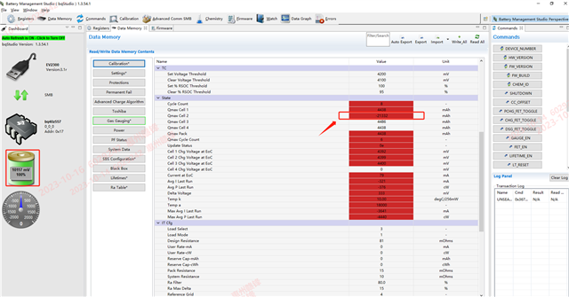
Please help analyze what is causing the abnormal change the capacity of the battery Qmax Cell2?
Attached the gg file and the figure.
Thanks
Star