This thread has been locked.

If you have a related question, please click the "Ask a related question" button in the top right corner. The newly created question will be automatically linked to this question.

TPS922055: Schematic Review

Part Number: TPS922055
Other Parts Discussed in Thread: TPS922052, TPS922053, TPS922054

Dear TI-

Could you review the attached schematic for the TPS922055 LED driver?

Thanks-

Mike Schell

LED Driver Schematic.pdf

  • Hi Mike,

    Please refer to the datasheet and change your schematic to the buck topology. (A screenshot is shown below.) You can then send me the schematic again. I will help review it.

    Best Regards,

    Steven

  • Hi Steven-

    Thank you. Here's the corrected schematic. Could you recommend some values for R1 and R2?

    Best Regards-

    Mike

    0447.LED Driver Schematic.pdf

  • Hi Mike,

    Please refer to my comments below:

    1. If max current of the LED is 1.5A, then TPS922052 / TPS922053 can already meet your requirement. There is no need to use TPS922055.
    2. If you do not separate the analog ground and power ground, then you can consider using WSON package for smaller size.
    3. For COMP pin, you can change the 1kohm to 0ohm. You can also leave a resistor footprint (NC) in parallel with the 1nF (the R_DAMP in Figure 9-1. 24-V Input, 4-A Output, 4-piece WLED, Analog Dimming Reference Design from the datasheet). You can refer to Section 9.2.1.2.5 Other External Components Selection from the datasheet for its usage. You can adjust the COMP pin components based on your test results.
    4. The 1uF between CSN pin and CSP pin is not needed.
    5. Based on my experience, the 10uF output capacitor is too large here and not needed. You can try 1uF + 100nF combination as the output capacitors and adjust their value based on your test results.
    6. I will create another reply to separately explain how to design the UVP resistor divider (R1 and R2 in your schematic) so that others will see this point clearly.

    Best Regards,

    Steven

  • Hi Mike,

    Below are some guidelines on how to design the UVP resistor divider:
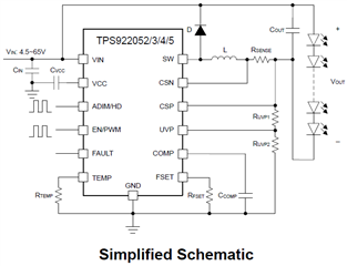
    1. The UVP pin of TPS922052 / TPS922053 / TPS922054 / TPS922055 has two thresholds,
      1. The first one is 1.4V. (Please refer to Section 8.3.6 CC/CV Charging Mode and Figure 8-5. CC/CV Mode Transition from the datasheet.) When the voltage of the UVP pin is above 1.4V, the output current won't be affected by the CV mode.
      2. The second one is 1V. (Please refer to Section 8.3.7 Fault Protection and Table 8-3. Protections from the datasheet.) When the voltage of the UVP pin is below 1V, "LED open load" protection will be triggered.
    2. To make sure your output current won't be affected in all working condition, you should make sure (Vin_min - Vout_max) * R_UVP2 / (R_UVP1 + R_UVP2) > 1.4V. 
      1. Vin_min: minimum input voltage
      2. Vout_max: the sum of the maximum forward voltage of each LED in the LED string at your maximum target output current
      3. R_UVP1, R_UVP2: Please refer to the below figure.
    3. Please do not design R_UVP1 and R_UVP2 with too small values. You can refer to this E2E thread for the reason. A rule of thumb is that you can design the sum of R_UVP1 and R_UVP2 to be around 1Mohm or 2Mohm and this normally would be a good start point. You can then adjust the values based on your test results.

    Best Regards,

    Steven

  • Hi Steven-

    Thank you, this is very helpful. I will implement your recommended changes.

    Best-

    Mike

  • Hi Steven-

    Thank you. As you already know, adding this info to the spec sheet would be great.

    Best-

    Mike

  • Hi Mike,

    You are welcome. Thanks for your advice and we will consider it in the next datasheet revision.

    I am going to close this thread. Feel free to contact me if you have any further question.

    Best Regards,

    Steven