Because of the holidays, TI E2E™ design support forum responses will be delayed from Dec. 25 through Jan. 2. Thank you for your patience.

This thread has been locked.

If you have a related question, please click the "Ask a related question" button in the top right corner. The newly created question will be automatically linked to this question.

TPSM63606: EMI performance of custom board worse than EVM kit

Part Number: TPSM63606

Hi,

We recently received our first batch of boards with the TPSM63606S chip and we are doing EMI tests with them. 
We also tested the EVAL board for this IC and were very happy with the EMI results it gave.

However, now with our custom board we are seeing a weird EMI signature in the lower frequency end. We don't think this is related to the rest of the circuitry on the PCB as we have removed everything else from the PCB apart from the TPSM63606S and it's required components plus the EMI filter. Our input EMI filter is the same as on the EVM board, even using the same inductor from CoilCraft.

I have attached a measurement report taken from the TPSM63606SEVM board and one from our custom board. As you can see, our custom board gives peaks between 150KHz and 200 KHz, while the EVM does not.
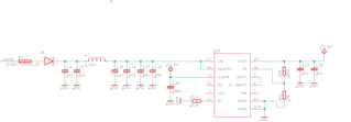
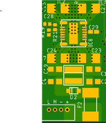
I have also attached screenshots of our schematic and board layout. In our opinion the schematic and board layout are super similar to the EVM module so we can't figure out what is giving us these high peaks.

Our module is set to output 11.6V with a 105k and 10k voltage divider. The frequency is set to 2MHz with a 6k34 resistor as recommended for a 12V output voltage by the datasheet.

We hope someone with more expertise in this subject is able to help us with this problem. Thanks in advance!
custom PCB.pdfTPSM63606SEVM.pdf

  • Hi Luca,

    Thanks for the inquiry. Looking at the tests I have some comments on your design. I'm assuming the test results are of conducted EMI plots.

    1. Your EMI filter is designed correctly with a cutoff frequency about a decade below your switching frequency so the peaks in 1-2MHz are mitigated properly.

    2.  With the peaks at the "lower" frequencies of 150kHz and less towards your switching frequencies of 2MHz, I suspect the noise to be common mode noise. 

    Some possible sources of common mode noise could be coupling to your load resistor to the testing plane. Do you have any pictures of the test setup?

    I would try twisting the load resistor in different orientations and height on the output. Or even elevating the board off the test bed at varying heights may reduce the common mode coupling, and in my experience, it will produce different results. 

    If there are some further issues, I will need to take a look at the layout also with the inner layers and layer stackup of the PCB.

    Regards,
    Henry

  • Hi Henry,

    Thanks for your reply. You are right, they are conducted EMI. Sorry for the confusion.

    We have currently measured with a LISN on the 24V input of the board. This LISN measures both differential and common mode noise. We also have a current clamp available so we can do some more measurements and differentiate between common and differential mode noise.

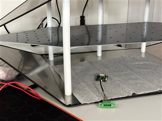
    We are testing the board by putting it into our TEM cell which is grounded to the same ground as the DUT. The DUT then connects to a 24V lead acid battery trough the LISN. Between the PCB and the TEM cell is a piece of cloth to prevent the bare PCB from being shorted on the ground plane. I have attached a picture for reference.

    We have tried different orientations and heights, but this made no noticable difference. 

    Can we share the details about the inner layers and stackup in a more private way?

  • Hi Luca,

    Sure, feel free to send the files via PM and I will take a more in depth look.

    Regards,

    Henry