Because of the Thanksgiving holiday in the U.S., TI E2E™ design support forum responses may be delayed from November 25 through December 2. Thank you for your patience.

This thread has been locked.

If you have a related question, please click the "Ask a related question" button in the top right corner. The newly created question will be automatically linked to this question.

UCC29950: EMI/EMC Issue with Charger Board

Part Number: UCC29950

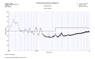
My team has designed a lead acid battery charger using the above part number. We used the evaluation board recommended parts and design. I attached the schematic below. my charger works, however I have EMC issue. As you can see from the attached Vertical SCAN it has major emission between 30 MHz-50 MHz and below 100 MHz in general as you can clearly see in the scan. I have tried ferrites with my AC wires to my board, it did not reduce the emission much. I also tried a mock up shield that did not help much as well.  I am wondering how to resolve this problem, I would appreciate any insight to this problem I am facing with my product. 

 AC-Rectifier-Circut.pdf

  • Hi,

    I have assigned this thread to product expert. He should get back to you asap.

    Regards

    Manikanta P

  • Hi Manikanta thanks for your quick response, we have few additional questions, one is we used two commons mode chock in the beginning of our circuit for the charger board as you can see from the schematic, the engineer who designed it is not currently with us and we are wondering why we needed to use 2 common mode chock and planning to by pass the second one that we think is contributing to the EMI problem we are having. let us know if you have any suggestion on the best way we can just remove it from the circuit. The part number of the common mode chock we are trying to remove is 744825605  

  • Hello Wosen, 

    I'll try to help you solve your radiated-EMI problem.  

    The best way to eliminate this problem is to suppress the noise at its source, but finding that source can be difficult.  It may be due to high-dv/dt from the PFC transistor or from ringing of parasitic inductances and capacitances around the switching components.  Some of the noise may come from the LLC section as well.   If you have access to EMI test equipment, you can use insulated current-loop "sniffer" probes and E-field antennas to hover near switching components (diodes and other power components, too) to track down the sources.  Noise can radiate from PCB tracks and loop areas as well as from cables, so don't forget to examine your board design for this.  

    From the EMI scan that you provided earlier, most of the noise is around 40MHz which has a period of 25ns, or about 12ns from negative peak to positive peak.    A possible source is the dv/dt of the PFC MOSFET which could change almost 400V in only 10ns or less. 
    The higher radiated frequencies (up to 120MHz) may be coming from ringing of parasitic L and C of components and pcb tracks.  

    In your schematic diagram, I noticed that the heatsinks H1 and H2 are grounded to earth-GND.  I assume H1 goes to the AC diode-bridge which is not a major noise source.  But H2 is probably cooling Q1 and D43, and high dv/dt from these parts may capacitively couple noise currents into earth-GND. 
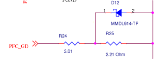
    As a test, I suggest to connect H2 to PGND and see how the noise signature changes.  Also check the conducted-EMI performance to make sure that does not get worse.   If you increase R25 value you can slow down the turn-on dv/dt to see if it helps reduce the noise.  

    I don't know why your previous engineer used two common-mode chokes in this design.  Maybe the single CM-choke was not enough to meet the conducted-EMI specification.  Why do you think L3 is contributing to the radiated problem?  But L3 is a 5mH choke whereas L2 is 1.2~2.4mH, so maybe you can consider to keep L3 and remove L2.
    It is simple to test the effects of removing either of these chokes.  Just short out their windings with pieces of wire (short pin 1 to 12 and 6 to 7 on L3, or short 1 to 2 and 4 to 3 on L2).  You don't even have to remove them from the board.  

    During EMI testing, is your charger packaged in a metal enclosure or is it an open board?  Metal boxes can contain radiation, but cover seams and ventilation slots can become tuned slot-antennas if their lengths and widths are not sized appropriately to suppress such radiation.  Please check your mechanical design for these details.  A board in a plastic box is basically an open board, so any radiation from an open board must be prevented at its source. 

    Regards,
    Ulrich

  • Ulrich,

    Thanks for your detailed response. The reason I thought L3 might be contributing to the radiated problem was that we used the sniffer prob to measure emission on a signal analyzer and we measured emission in the same frequency range we are seeing them at MET LABs. I also measured the total wire length in the chock and it happened to be very close to the quarter wavelength of our 30-50 MHz emission so I taught it might be acting as an effective antenna. I shorted the L3 and tested it again and the emission did not improved so it is safe to rule out the common mode chocks. We were wondering how all of the heat sinks was registering high emission on a sniffer prob measurements. Your suggestion that "A possible source is the dv/dt of the PFC MOSFET which could change almost 400V in only 10ns or less." is holding more weight for me as possible source of emission now. How high can we increase the value of R25. and can you be specific on the relationship of R25 and the switching time?. Our enclosure is metal which is grounded to earth ground so your hypothesis that the PFC MOSFET may capacitively couple noise currents into earth-GND might hold true. Need carefully designed tests to test your hypothesis, I am open to suggestions. 

    Regards,

    Wosen 

  • Hello Wosen, 

    Thank you for the additional information on your EMI testing. 

    My experience with EMC-related noise suppression is limited, mostly to conducted-EMI reduction, very little with radiated emissions.  My debug advice is mostly based on general principles and largely involves trial-and-error testing.  Determine a list of suspected causes, make a change that you think should affect the noise and test to see if the change helped or hurt the emissions.  Always make only one change at a time, and if they are independent changes, restore the previous configuration before making a different change. 

    That said, to test if the heatsinks are conducting noise into the earth-GND, I suggest to disconnect them and insulate them from GND_EARTH.  Try a test with them left floating (electrically unconnected to anything), then if electrically-connected to PGND, then if connected to BULK_HV.  Assess the result of each proposed test to see if they are favorable or unfavorable before proceeding to the next test.   

    If a favorable result solves all of the problem, then decide how to implement it into production.  If it improves the noise only partially, then try the other test options to see if they may be more favorable or not.  Then keeping one or two favorable configurations, try making other changes that could improve the emissions even further.  

    Increasing R25 will slow only the turn-on dv/dt of Q1.  Increasing R24 affects the dv/dt of both turn-on and turn-off, but mostly turn-off.  Adjust one or both resistors in small increments one change at a time and assess the results before making the next change.  The dv/dt of the drain voltage (Vds) of Q1 is determined mostly by how much current is allowed to flow through the MOSFET's Crss.   That current is controlled by the gate resistance and the peak current capability of the MOSFET driver.   

    The UCC29950 datasheet does not specify the peak PFC_GD current, but it can be estimated from its rise time spec: Ipk = 1nF*0.6*12V/30ns = ~0.24Apk.
    This peak current times the series resistance R24+R25 gives a voltage drop across the resistors.  With original values, this Vdrop = 0.24A*5.2R = ~1.25V. 
    With a 12-V output range for PFC_GD (assuming VCC = 12V), this small voltage drop has no influence on the turn-on dv/dt of Q1 because all of the peak drive current is available to flow through Crss while Vds is falling from ~400V to 0V.  To slow down the dv/dt, you need to choke off the gate current through Crss.   So R24+R25 must be increased to the point where the gate-drive current is reduced.  

    Q1 Vds will not start falling until its Vgs has reached the turn-on threshold (typically around ~5V).  All of the gate current goes to charging Cgs (Ciss) until it hits the so-called Miller plateau at ~5V, then Vgs stops rising and all of the gate current goes into Crss as the drain voltage start falling.   Since the gate-drive voltage difference is now about 12V-5V = 7V, you can increase R25 only (to keep turn-off timing the same (for now)) to 32R to reduce gate current from 0.24Apk to ~0.2Apk  ( 7V/ (3R +32R) = 0.2A ).  This ~17% reduction in gate current should result in a 17% reduction in dVds/dt. 
    Note that the reduced gate current also slows down the charging of Ciss, so the FET has a longer time delay before the Miller plateau is reached at each turn-on.  

    This is the principle for dv/dt control of Q1, and similar math can be done to size R24 for slowing down turn-off.  Note that the EMI noise comes from +/-dv/dt, but changing R24 and R25 can affect not only the dv/dt's but also the on/off time delays which do not affect EMI, but may affect other control aspects like peak current limit, etc. 

    Regards,
    Ulrich

  • Ulrich,

    We changed R25 to 33 ohm and we saw a reduction on our emission. we then  changed it to 1Kilo Ohm and we saw significant reduction in EMI when which were charging <4A current. when we charge with <7A current firmware R18 blew up. can you help us understand why that is. We understand 1K could be too much of a change bet why id it work one setting and not the other?

    Regards,

    Wosen

  • Hello Wosen, 

    Thank you for your update of the situation.  
    I don't know why changing R25 to 1kR would result in blowing up the current-sense resistor R18. 
    Failure of R18 would be from excess power loss, and that comes from excess current which comes from excess on-time. 

    1kR gate drive would significantly slow down turn-on of the MOSFET, but not the turn-off, so I would expect less current in the inductor.

    Are you sure that you changed R25 and not R24?  1kR at R24 would slow down turn-on AND turn-off and that could allow too much current to build up.
    And it would reduce dv/dt on both edges of the drain voltage (maybe accounting for the low EMI).  Please verify which resistor was changed. 

    If it truly is R25 that is changed, please examine the inductor current (using the <4A control) to see what effect a 1kR turn-on has on the current.

    Regards,
    Ulrich

  • Hello Ulrich,

    I reworked the charger with R24 = 240 Ohm and R25 = 180Ohms, we got a very encouraging results (using the <4.5 A control). However when I reworked the charger with R24 = 1.3 KOhm and R25 = 1KOhms the current-sense resistor R18 blow up. I am trying now the optimum combination of the two resisters to pass my EMC Test without compromising the working of my charger. I am open to suggestions.

    Regards,

    Wosen 

  • Hello Wosen, 

    I'm sorry, I was not clear in my previous questions and suggestions.  I do not recommend using any high-value resistances in the gate-drive path of Q1.

    Since D12 blocks turn-on gate current, the turn-on time of Q1 is determined by the sum of R24 and R25. 
    Since D12 passes turn-off gate current, the turn-off time of Q1 is determined only by R24.  

    Because of this asymmetry, if R24 >> R25, then turn-on and turn-off dv/dt will be about the same rate, although one is positive (rising dv/dt) and one is negative (falling dv/dt).   If R24 = R25, then turn-on dv/dt will be ~1/2 of turn-off dv/dt.  If R24 << R25, then turn-on dv/dt will be << turn-off dv/dt.

    The first design concern should be for reliable operation, regardless of EMI.  You can't allow the worst-case stresses on Q1  and R18 to be so high that they are in danger of failing.  In my view, slow turn-on and slow turn-off may be good for EMI, but bad for reliability.   Also, I think that slow turn-off may be worse than slow turn-on.  

    So the values for R24 and R25 must be chosen first to ensure reliable long-term operation of the Q1, R18, and other components, and only secondly to help reduce EMI. Your original gate-drive design had 3R and 2.2R which resulted in good operation but poor radiated-EMI.  
    I suggested to reduce dv/dt with increased gate resistance, but to change the values in small increments and reassess operation. 
       
    I also suggested to re-evaluate the way the heatsinks are grounded and try other connections to them. I don't know if you tried this or not. 
    You reported using 33R at R25 and that helped the EMI.   Using 1kR at R25 improved EMI even more, but blew up R18 at high current. 
    That did not make sense to me, so I asked you to verify if you changed R25 or R24.  I did not get an answer to that. 

    In any case, my expectation is that any R-value > 100~150R is probably going to slow down turn-on or turn-off (or both) too much and result in higher switching losses in the MOSFET.  EMI may be better, but Q1 may be overstressed and unreliable. 
    If R24 is too high, the MOSFET turn-off will be very slow and inductor current may increase higher than expected.  This current flows through R18 and may overheat it, causing it to fail. 

    My main point, then, is that there is a limit to how much R24 and R25 can be increased to reduce EMI before they start to reduce reliability.  
    At that limit, you must use other means to further reduce EMI, because you can't sacrifice reliability for EMI.  
    Changing the values of R24 and R25 are very simple low-cost means to reduce EMI, but once system reliability becomes affected, only less-simple, higher-cost solutions can be used. 

    I recommend that R24 + R25 < 100R total, but even that sum may be too high if losses in Q1 and R18 become too great for long-term reliability. 

    Regards, 
    Ulrich

  • Hello Ulrich,

    We tested isolating the earth ground connection including the heat sink and made it floating and we didn't see any improvement on the emission.

    However I did used 33R at R25 without changing R24 and we did see an improvement on the emission.

    I understand your explanation that increasing R24 and R25 to too high values might cause a reliability issue and I definitely don't want to scarifies reliability for EMI.

    I tested the charger with 2 different combination of high value resisters with both failed. 

    1. R25 = 1KR and R24 = 3R 

    2. R25 = 1KR and R24 = 1.3KR

    both of the above combination failed.

    what way did you calculate the worst-case stresses on Q1  and R18?

    Regards,

    Wosen

  • Hello Wosen, 

    Thank you for the additional information. 

    If you review my text above, I suggested not only to try disconnecting the heatsinks from earth ground, but also to try connecting them to PGND or to BULK_HV. 

    It is interesting to me that R18 fails when R25 = 1KR which affects turn-on dv/dt.  I would not expect that.  
    Please check to see if D12 is installed in the polarity as shown in the schematic diagram.  If it is installed backwards, it would make R25 slow down turn-off dv/dt, which is what I expect might cause R18 to fail.  If D12 is installed properly as shown, then I have to admit that I don't know what is causing the R18 failures.  

    I did not make any stress calculations for Q1 and R18.  I made some general statements that high values for R24 and R25 will lead to stresses on Q1 and R18.  The actual stresses need to be assessed by examining the voltage and current waveforms across and through these parts.  Actual power loss can be calculated from these waveforms.   Compare stresses in the modified design (lower EMI, but possible increased risk of failure) to stresses in the original design (with excess radiated-EMI) to decide how much value change is allowable.   

    Regards,
    Ulrich

  • Hello Ulrich,

    Connecting the heatsinks to PGND would not work in our design because PGND is at much higher voltage than earth ground to be specific 50 V higher therefore, it is not ideal to connect the heat sinks to PGND.

    We will check for the orientation of D1 and We will also compare the stresses in the modified designs and CircleBack to you with any further questions we might have. 

    Regards,

    Wosen

  • Hello Wosen, 

    I suggest that you can try connecting the heatsink to PGND as a test to see if it has any beneficial effect on the radiated-EMI.  It does not have to be a permanent change.  Also, try to BULK-HV.
    If no significant improvement is measured, then at least that possibility has been explored and closed.  If there is an improvement, then you may consider whether to pursue further investigations into where the heatsink(s) can be connected or not, to control the noise current path(s). 

    Regards,
    Ulrich

  • Hello Ulrich,

    We tried 3 chargers with the followings changes to R24 and R25

    1.  R24 = 3Ω and R25 = 2.2Ω (which is the bassline as it is in the original unmodified board)

    2.  R24 = 56Ω and R25 = 43Ω

    3.  R24 = 240Ω and R25 = 180Ω

    we monitored charging current around 4.5 A for all three and we where measuring the temperatures of the heat sinks and anther transformer.

    we learned that configuration 3 had temperature rise which is the same as the baseline around 53-55 C both at the heat sink and at the transformer.

    however configuration 2 has the heat sink at 65-75 C at the heat sink and  around 120 at this transformer which is too hot.

    I tried configuration on 2 different boards and got the same temperature measurements. 

    I can't send the schematic over here since this is a public form. But I can send it to you privately so that you can see which transformer I am talking about.

    Regard,

    Wosen. 


  • Hello Wosen, 

    I have sent an email to you so that you can reply with your schematic file in private. 

    For the 3 cases above, #1 (the baseline original design) has a radiated-EMI problem.   Do both cases #2 and #3 solve the EMI problem, or only one of them, or neither completely solve the problem?  I'm not sure what the situation is, since we seemed to have moved from an EMI issue to a thermal issue.

    As an aside note: if the transformer temperature rise in case #2 changes from ~55C to ~120C, then some serious changes of waveforms must have occurred.
    Roughly speaking, for the temp rise to double, the total power loss must double, and transformer loss is the sum of core loss and copper loss. 
    You can determine if the increased loss comes from higher Irms alone or higher delta-B alone or a combination of the two, only by examining both current and voltage waveforms at the transformer.  

    In general, I find it difficult to assess whether the advice that I'm giving you is leading in the right direction or not. I have made many suggestions about changing values, changing connections, checking polarity, etc. but I don't receive much feedback on which of the suggestions you have tried and what the results were, and which ones you declined to try. 

    For me to help you more effectively, I need to know whether my suggestions and observations make things better or worse.

    Regards,
    Ulrich 

  • Ulrich,

    Sorry to add the thermal problem to the EMC trail we have here. But, I was just testing the reliability of the charger to see the effect of changing the R25 and R24. Thermal problem might be a set up problem but I found out that it is not related to the EMC problem.

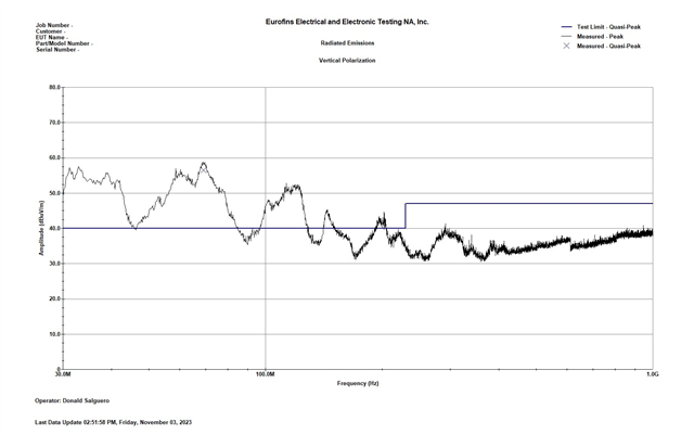
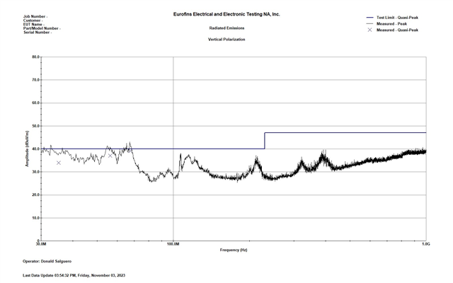
    TO answer your question set up #2 improved our EMC slightly, dropped it roughly by 10 dBm however set up #3 almost dropped it by 20 dBm which is significant and made us pass class B limits by 1 dB. I attached the open air vertical measurements with our baseline #1 on open air measurement and  our modified #2 with 3 ferrites clamp on AC line

               Figure-1  baseline #1 on open air measurement 

    Figure-2 #3 on open air measurement

  • Thank you, Wosen, for closure on this issue.  

    I hope the EMI solution does not cause significant other problems as a side-effect.

    Good luck with your development.
    Ulrich