This thread has been locked.

If you have a related question, please click the "Ask a related question" button in the top right corner. The newly created question will be automatically linked to this question.

TPS54331: Failure of 24V-to-3.3V circuit.

Part Number: TPS54331


Hi,

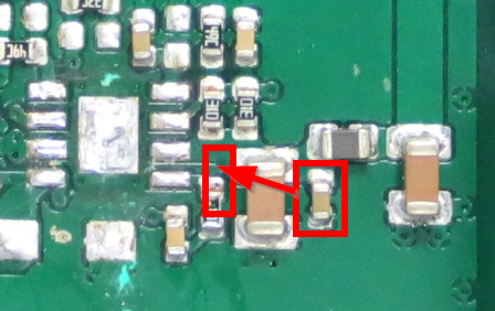
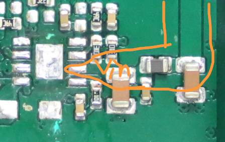
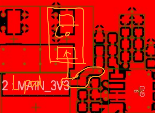
We’ve had 4 instances now with our product in a particular geographical location whereby the 3.3V supply circuit has failed. On review of the failures, the catch diode has failed short and, in 3 units, the TPS54331 was also faulty (had to be replaced).

Units have been running for a few years and then fail. Units are operated 24/7 but may be power-cycled during maintenance of other equipment at the location. We are trying to determine if there is any link between the maintenance activity and the failures but this is not yet forthcoming.

The same product is used world-wide and we’ve had no reports of failures from any other location.  We would like to determine the cause of this failure or if there are any tests we could do to replicate the failure.

The attached document shows schematics and PCB layout.  I've also attached some Webench designs that were done at the time of product development and a spreadsheet of calculations.

Thanks,

Kieran


Failure of TPS54331 circuit.pdf24V-to-5V at 0.5A using TPS54331DDAR (TI Webench design #73 - 28-Mar-19).pdf24V-to-3V3 at 0.5A using TPS54331DDAR (TI Webench design #72 - 28-Mar-19).pdf24V-to-3V3 at 1.5A using TPS54331DDAR (TI Webench design #73).pdfDesign Calcs for 24V-to-3.3V using TPS54331.xlsx

  • Hello Kieran,

    Thanks for reaching out!

    I think you should look at Vin phenomenon, check whether has voltage spike during operation.

    1. This rail (U902) input trace is placed before Cin bulk cap, not after Cin, here the Vin hasn't been well filtered. If there's voltage spike larger than recommended 28Vin_max or ABS 30Vin_max, device possibly could damage.

    2, The small input decoupling cap should be placed near Vin-pin as close as possible, to filter input high-frequency noise.

    3. Please enlarge the Vin trace, use a large polygon to decrease the trace impedance.

    4. The FB sensing trace should connect to the Vout after Cout, not before Cout (inductor pad), to get a clean Vout signal.

    For further debugging, please capture Vin/SW/Vout/IL waveforms, check whether has OV/OC risks.

  • Hi Miranda,

    Thanks for the reply.

    I guess you suspect the input is experiencing an over-voltage condition for some reason.

    The input is protected somewhat by the transient suppression diode (SMD part shown to the right of the fuse).  However, on review of this part, we see that it has a clamping voltage rating slightly higher than the recommended 28Vin_max of the regulator.

    Lastly, the curious thing about this board is that the same regulator is used in two circuits, a 3.3V and a 5V circuit.  However, only the 3.3V circuit fails, we've had no failures of the 5V circuit.  The 5V circuit is shown above the 3.3V circuit in the first image.

    Regards your comments . . .

    1. There are two sets of bulk capacitors shown in the images.  Each regulator circuit has two 10uF ceramic capacitors (Cin) with a ferrite bead between them close to the input pin.  The two large electrolytics on the right are bulk capacitance for the rest of the board.

    Is this OK?

    2. The small input decoupling cap was added as a precaution but was not present in the Webench design.  Agree this could be placed closer to the input pin.

    3. The input trace width was dictated by the width of the ferrite bead, I guess it could be increased.

    4. Yes, could move FB trace to after Cout but it would still be very close to inductor pad (as they share the same copper).

  • Hi Kieran,

    Glad to see you have found the root cause related to input overvoltage.

    I think the reason why only 3.3V rail fail, 5V rail normal could be: a) 3.3V Vin trace is placed closer to system Vin, while 5V input trace is placed after a bulk cap, maybe 3.3V rail is more over-stressed; b) 3.3V rail loading is 1.5A max, higher than 5V rail loading 0.5A max, I guess the higher current will easier to break SOA curve max power limit and cause device damage.

    About how to select Cin, I don't know your application conditions, cannot give a recommended value directly. But I think you could modify the board Cin components, and check whether within normal Vin range.

  • Hi Miranda,

    I can't say as yet that input over-voltage is the root cause.  The reason for this is that the 5V regulator has not been damaged and both regulators have the same input circuit/components and very similar PCB layout,  The 5V input trace is not placed after the bulk cap.  Both inputs share the same wide copper trace from the boards bulk capacitors.

    For sure, a high enough input voltage will damage the part so input over-voltage may be the cause but I cannot as yet determine why this would happen.  

    We will investigate further.

    Regards,

    Kieran

  • PCB layout and input components . . .

  • Hi Kieran,

    Sure, look forward to your test progress, let me know your further support need.