This thread has been locked.

If you have a related question, please click the "Ask a related question" button in the top right corner. The newly created question will be automatically linked to this question.

UCC28950: Issue in PSFB Converter using 28950

Part Number: UCC28950

Hi all,

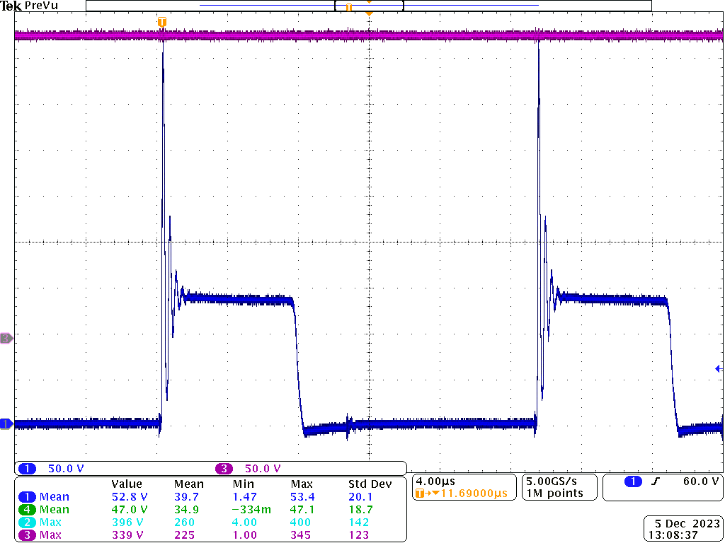
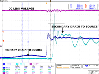
I trying to implement PSFB converter with UCC28950 IC. I am giving 12V bias separately and the input voltage(400V) through a Bridge Rectifier Circuit.

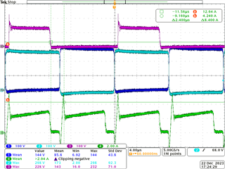
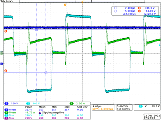
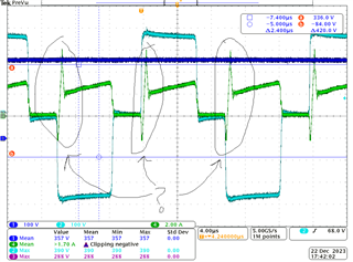
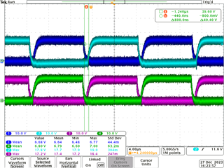
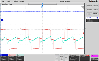
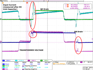
When the bias 12V is given, the QA, QB, QC, and QD are showing pulses of nearly 50% duty ratio. However there are no pulses for switching the secondary devices (QE, QF).

The Vref value is 5V, SS/EN is also 5V.

What could be the issue for the circuit not turning on.

What other parameters need to be checked for troubleshooting.

Thanks 

  • Hello,

    Your inquiry is under review and I will get back to you shortly.

    Regards,

  • Hello,

    I actaully made a mistake in my calculations based on previous information.  The clamp would have been set at 218 V roughly.  However, your latest information is based on 54 V output and not 48 V. 

    So the clamp would be at a different voltage would ber 

    Vclamp = (Iout +dIL/2)*R8 + Vout*2 + VD6

    dIL = 6.25 A according to your excel file.

    Iout = 450W/54V = 8.33A

    Vclamp = (8.33A +6.25A/2)*(10 ohm)+54*2+1.5V = 224V

    If CH1 is 50 V per division the voltage rings up to roughly 430V.  This would indicate the clamp is not working the way it should.

    You might want to check the voltage across R8 to see if it is indeed 54V*2 = 108 V.  Capacitor C1 may not be connected or damaged.

    If the voltage across C1 is correct you may want to check R8 to make sure that it is not damaged.  Lastly you may want to check the SR FET drain current to make sure it is what it is supposed to be.

    Regards,

  • Why is there need for both clamp (R-C-D) and snubber (R-C) circuits in secondary side. 

  • Hello,

    I am reviewing your inquiry and will get back to you shortly.

    Regards,

  • Hello,

    The RCD clamp will clamp the spike on the drain of the SRs to protect the FET.

    The RC snubber across the FET will be used to damp the ringing across the SR.  This will help with EMI if you decide to use it.

    Regards,

  • Hi Mike,


    Thanks for the reply. I have measured the secondary inductance on the transformer and its coming to be around 1uH on one half and 0.5uH on the other. Is this reason for the huge spike.

    Also based on the calculations given for flyback RCD Clamp as per

    RCD_CLAMP.pdf

    I am using the following values (as upper case for Voltage of 54V, Ipeak of 15A)

    RCD CLAMP.pdf

    I am getting around Rclamp of 1kOhm, the value of capacitance of 56nF and Power dissipation of 30W (for a peak current of 15A).

    If I increase the peak current to 25A. I am getting loss at 86W.

    So what should be reasonable loss in clamp for a 1500W system. and what should be reasonable leakage in secondary halves and ideal winding arrangement for centre-tapped systems.

  • In continuation with above post. Today I tested with RCD Clamp with R=550Ohms, C=0.094uF (Though this was obtained for clamping at 230V, with leakage as 2uH)

    The transformer was also changed to ETD49 with primary magnetizing inductance as 3mH. The leakage measured is (Secondary half 1:  464nH and Secondary Half 2:  765nH).  The waveforms obtained are attached.

    There is only one peak which is very sharp at around 350V rest of the waveform is getting clamped around 250V.

    My queries are

    a) Is this a single 350V peak (measurement error)? Nevertheless, the snubber resistance started heating (the power of snubber resistance is around 15W, The calculated value is ).

    b) Will the Loss in the RCD clamp reduce once Synchronous Rectification is enabled? So should I proceed with testing at higher power levels? Presently its around 450W. I need to test at 1500W.

    c) What is the preferred winding arrangement? I am using (Primary Half (15 Turns), Secondary 2 (6 Turns), Primary Half (15 Turns), Secondary 1(6 Turns) with the secondary (S1) closest to the core limb). The primary halves are connected in series. 

  • Hello,

    I am reviewing your inquiry and will get back to you shortly.

    Regards,

  • Hello,

    Diode D4, D6 and R8 will dissipate all of the leakage energy from the secondary leakage inductance (Lslk).

    The following equation will estimate the power dissipation of the leakage inductance (Pslk).

    Pslk= ((Lslk/2)*(Iout)^2)*fsw

    Regards,

  • HI Mike,

    At what load % should the synchronous rectification be enabled. Say if full load is 1500W. At what load should the synchronous rectification be enabled.

  • Hello,

    The DCM comparator is used turn off the SRs based on loading.  You should turn off the SRs before the inductor current goes discontinues to protect the FETs.  Application note slua560 has a section on where to set the DCM threshold based on inductor ripple current and loading.  The following link will bring you to the application note.

    https://www.ti.com/lit/pdf/slua560

    Regards,

  • Hi Mike,

    Sorry for the late reply. During the testing the devices got damaged twice. In one instance the clamp diodes D4 got damaged. I had used 600V,3A SMD ultra fast diode. However, Now i have used 600V, 6A diode with TO-220 Package. Now i am able to get regulation at 48V with input around 330 onwards. However, I am confused whether the delays are correct and whether softswitching is happening. The switching frequency is reduced to 50kHz

    Ch 1: Drain to Source Voltage Primary Device, Ch 2: Drain to Source Voltage Primary Device

    Ch 3: 100V scale: Secondary Drain to Source Voltage, Ch 4: Input Current

    Ch 1: Input Voltage , Ch 2: Transformer Primary (CYAN)

     Ch 4: Input Current

    Is the transformer waveform correct? 

    How do we see if soft-switching is happening , if we don't have access to switch currents.

    what should a DESIGN_1500W_48V_22_12_2023_NEW_CONTROL_CARD_UPDATED_LEAKAGE.xlstypical delay be set. I am presently using the following design values as per attached excel sheet.

  • Hello,

    Your inquiry is under review and I will get back to you shortly.

    Regards,

  • Hello,

    The excel tool will give you the initial delay settings.  I would suggest loading the supply at 10% and fine tune the turn on delays.

    The following link will bring you to an application note that describes how to setup the timing.

    https://www.ti.com/lit/pdf/slua560

    The current in your transformer does not look correct.  Maybe the timing in the SRs is off.  First try to disable the SRs to see if the transformer current improves.

    Regards,

  • What should be the expected shape of the current

  • Hi Mike, 

    I have captured the waveforms, as attached.


    The Delay was kept fixed by keeping KA=0. Also, RDELAB=36k, RDELCD=36k, RDELEF=14k

    Drain_Source_voltage.pdf

    Is the switching correct.

  • The value of RDELAB and RDELCD and RDELEF is increased to 47k, 47k and 23k Respectively

    The gate waveforms of primary side is shown below

    The current waveform is still showing spike after increasing delay also

    Ch1: Q2 Drain, Ch2: Current,Ch3: Transformer,Ch4: Secondary QE GATE

    After disabling synchronous rectification, there is still spike in the current waveform, I am attaching the waveform

    This is after disabling SR more (DCM pin connected to VREF).

    The EVM module from TI is having the following waveform

    what else should be checked to resolve current spike.

    Thanks

  • Hello,

    I am reviewing your inquiry and will get back to you shortly.

    Regards,

  • Hello,

    Your waveforms look like that the SRs ore not turning off where they should.  That is why you are seeing the spike in current.

    If the SR driver is disabled you should not have an out E or out F.   Your waveform is still showing OUT E is present. If you disable the SR drive I believe the spike should go away.  Also adjust the E and F timing so it turns off during the FET free wheeling period will remove the current spikes as well.

    Regards,

  • Thanks Mike for your support even though its Christmas season.

    I have a doubt regarding the TABSET and  TAFSET calculations. In order to simply the issue of this peaky current , I thought I would increase the TABSET , but keep it fixed. So used a value of 47k for both RDELAB and RDELCD=47k. Shorted ADEL and ADEL to ground. 

    The input current spikes did not go. Also now there is some notches in transformer. 

    SCHEMATIC_LAYOUT_PSFB.pdf

    The value for RDELEF was chosen as 24k. However based on the equations in the datasheet.

    I am getting

     ns

    when RAB=47k , KA=0,CS=0;

    For TAFSET i am getting

     ns

    REF=RDELEF=24k

    Even if i use REF=90k (the allowable range mentioned in the datasheet is 13k to 90k), the max delay is 166n.

    So how do i set TAFSET=0.5*TABSET. iF the TABSET is 900ns .

    Is there anything else in equation which i am missing.

  • Hello,

    Were you able to disable the E and F FETs to verify if the issue went away?

    Regards,