This thread has been locked.

If you have a related question, please click the "Ask a related question" button in the top right corner. The newly created question will be automatically linked to this question.

UCC28950: Issue in PSFB Converter using 28950

Part Number: UCC28950

Hi all,

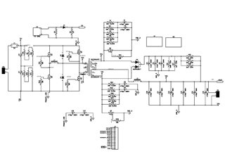
I trying to implement PSFB converter with UCC28950 IC. I am giving 12V bias separately and the input voltage(400V) through a Bridge Rectifier Circuit.

When the bias 12V is given, the QA, QB, QC, and QD are showing pulses of nearly 50% duty ratio. However there are no pulses for switching the secondary devices (QE, QF).

The Vref value is 5V, SS/EN is also 5V.

What could be the issue for the circuit not turning on.

What other parameters need to be checked for troubleshooting.

Thanks 

  • Hello,

    I am reviewing your inquiry and will get back to you shortly.

    Regards,

  • Hello,

    Do you have a schematic that I can review?

    Regards,

  • The Daugther board is oriented so that the pin matching occurs between that in power board and daughter board. 

  • Hello,

    I am reviewing your inquiry and will get back to you shortly.

    Regards,

  • Hello,

    I reviewed your schematic and it looks like the SR FETs will not be driven in the peak current sense signal is greater than 0.641 V.

    This is based on the voltage set at the DCM pin.

    You might want to to study the error amplifier output, CS pin, DCM pin and Out E pin to see why the SR drivers may not be getting activated.

    Regards,

  • Thanks, Mike for the reply. On going through the design document, a few doubts have crept up. For pins ADEL and ADELEF resistor network, Vref is connected as per the Excel design tools diagram. But in the application note SLUA16D, CS output is connected to ADEL, ADELEF resistor network.Which is preferred/correct for initial troubleshooting and for the final version.

    Also Even if the synchronous rectifier switches are not working, the secondary load voltage should be generate. In my prototype, the secondary voltage is also zero, is it possible that the transformer winding polarity is causing this issue.

  • Hello,

    I am reviewing your inquiry and will get back to you shortly.

    Regards,

  • Hello,

    Can you send me a link to the application note that you are discussing?

    Regards,

  • Hello Mike,

    There was gate driver issue which was sorted. Now the switches are being driven by pulses. However, there is still negligible output at around 100V. Also the transformer is making some sort of clicking noise. I am attaching the waveform observed in AC side of primary transformer

    It seems to operating in burst mode. However, why are the pulses bipolar.

    The reference document is attached. Here the DCM connection given is different from that mentioned in the excel tool diargram.

    6874.ucc28950.pdf

  • In continuation with above. It seems, for when the Input DC voltage is low (20V input) the system is operational (all four primary devices) pulses are there contin 
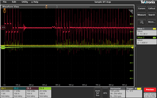
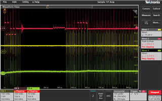
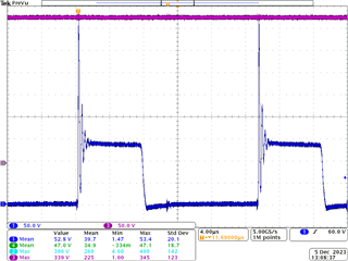
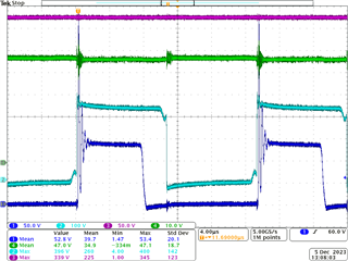
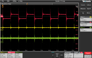
uously. After that it goes into some burst mode or some protection mode. 

    After the input voltage increases beyond say 35V. it happens to be in burst mode/protection mode.

    What should be the signals I should check for trouble shooting this issue

  • Hello,

    I am reviewing your inquiry and will get back to shortly.

    Regards,

  • Hello,

    The design is probably audible because it is bursting.  The bursting could be caused by a loop stability, noisy CS signal or poor layout.

    The following link will bring you to an application note that you can use to help review the design.  It goes through the step by step design process of using the UCC28950 in a PSFB.  Within the application note there is an excel design tool that can help you review the design as well.  

    https://www.ti.com/lit/an/slua560d/slua560d.pdf

    The information in the application note was used to design the 600 W evaluation module, TI part number UCC28950EVM-447.  You can find the user's guide for this evaluation module in the below.  There are waveforms and performance data that you might find useful in the User's guide as well.

    https://www.ti.com/lit/ug/sluu421a/sluu421a.pdf

    It might be worth your while to order the 600 W evaluation module to evaluate it.  You can use it to compare waveforms in your existing design and can find it at the following link.

    https://www.ti.com/tool/UCC28950EVM-442?keyMatch=&tisearch=search-everything&usecase=hardware&login-check=true

    After checking the design with the application note/excel tool, If everything is O.K.  you can start to trouble shoot the design.

    Troubleshooting your design.

    1.) You could have a voltage loop instability.  Start by checking this with the excel design tool to see if your theoretical compensation is correct.

    2.) Start by evaluating your design up at a light load with SRs disabled.  

         a.) This can be done by tying the DCM pin of the UCC28950 to the UCC28950 Gnd pin.

    3.)  I would monitor the UCC28950 's voltage amplifier output, CS pin,  SS pin and the primary of the transformer with a differential probe.

        a.) Start at 10 % load check for: 

             - Voltage amplifier output stability

             - Check to make sure the CS signal is clean without noise

             - Make sure the design is not going into over current hiccup mode protection.  The following section from the data sheet explains the cycle by cycle               and hiccup mode over current protection and how it works.


    4.) Once you have the design working at light loads you set the delay timing based on the application note discussed above.

    5.) Once the timing is set you could bring up the design slowly to see if works at greater loads and trouble shoot as necessary.

    6.) Once the design is working without the SRs, you can enable the SRs and bring the design slowly up again from light load to full load slowly.

    Regards,

  • Thanks Mike for the reply. I will update you based on the procedure suggested by you.

    Also I would like to know whether for initial startup (a) we can initially give the 12V bias to the IC and then ramp the input voltage from 0 to 400V .

    (b) Or should we set the voltage at 400V and then apply the 12V bias.

    Presently I am following method mentioned in (a)

  • Hello,

    I am reviewing your inquiry and will get back to you shortly.

    Regards,

  • Hello,

    What is the minimum input voltage or your design?  That is probably the input voltage you should start with.

    You can bias the IC with a separate bias supply. This is commonly done when troubleshooting designs that use a bias winding or a separate bias supply to power the PWM while doing initial troubleshooting.

    Regards,

  • Hi Mike,

    Thanks for the reply. I tried to modify the PSPICE simulation based on the values obtained in TI-EXCEL tool. However, the start up simulation is not working . The reference given is for 48V but it limits to 12V.

    Please suggest what changes are to be done for an output of 48V with 1500W power requirement.

    DESIGN_1500W_48V_Updated_02_11_2023.xlsUCC28950_PSPICE_TRANS.rar

  • Hello,

    I am reviewing your inquiry and will get back to you shortly.

    Regards,

  • Hello,

    Just checking.  Did the simulation work before you modified it?

    Regards,

  • Hello,

    After reviewing your inquiry again.  It looks like the model is working and the output is locked at 12 V, when your design requires 24 V.

    I think you may have one or two issues going on.

    1. The voltage divider from Vout to EA + not be setup correctly.

    2. Your transformer turns ratio is not set correctly.

    I would check these two items and adjust if needed.

    Regards,

  • Hi Mike,

    In order to test the system, I have changed the sense resitor to get a voltage of 24 V in output. I am  attaching waveforms captured in attached pdf. The load resistance presently used is 4 Ohms. The transformer primary inductance is 2.6mH and leakage inductance is 7uH. I am not using any shim inductance.

    The final requirement is 1.5kW at 48V.

    The key observation is that the transformer voltage is nearly square wave. Once system reaches 24V, any further increase in input voltage the system goes to burst mode.

    Also it is observed that the Gate Voltage of QA starts dipping and then nearly turns of as the system output voltage reaches 24V. I am also attaching updated daughter board schematic values

     Experimentation_notes.pdfPSFB_DAUGTHER_BOARD_09_11_2023.pdf

    I have tied the DCM pin to Vref to disable the outputs to QE and QF.

    How to tune the compensator or is there anything else missing/required to be checked.

    In simulation I am able to get nearly put 28V at input of 200V, however the simulation is painfully slow. Is there a method to speed up the simulation in PSPICE or what should be adjusted in compensator to speed up the tracking.I am attaching the simulation schematic.UCC28950_START_UP _PSPICE.pdf

    Please suggest what should be done with respect to troubleshooting the issue. Please note that I am measuring through differential probe with 100x attenuation so there is noise in especially low voltage signals.

  • Hello,

    I am reviewing your inquiry and will get back to you shortly.

    Regards,

  • Hello,

    Your simulation file is setup with a resistor divider that will set the output to 30.86 V.  So if you are trying to get 48 V in your simulation this will need to adjust this resistor divider,  UCC28950_START_UP _PSPICE.pdf

    The transformer turns ratio in your simulation if 5.25.  At 200 V the maximum output voltage achievable would be 200/5.25 = 38 V.  If this is the transformer turns ratio in your design, 48V will not be achievable at 200 V.  So your transformer turns ratio is not correct and will need to be corrected.

    The following link will bring you to an application note that reviews a step by step design process for designing a phase shifted full bridge converter (PSFB) using the UCC28950.  It will give you calculations for selecting the transformer turns ratio, loop compensation; as well as setting up the components around the UCC28950.  It also has a link to an excel design tool that uses the same calculations.  

    https://www.ti.com/lit/pdf/slua560

    This application note was used to design the UCC28950EVM-442 600 W evaluation module.  The following link will bring to the user's guide for this evaluation module and there are some waveforms in the user's guide that you may find useful when evaluating your design.  It may be worth while for you to order the evaluation module to evaluate the performance of the design.  You can compare this design to your design and it may help in the troubleshooting and design process. 

    https://www.ti.com/lit/pdf/sluu421

    https://www.ti.com/tool/UCC28950EVM-442?keyMatch=UCC28950EVM

    At this point I would recommend using the application note and excel design to double check your design.   You may want to work with the PSpice simulation to trouble shoot your design with the calculated parameters just to make sure everything is working before modifying your design.

    When it comes to simulation if you want to speed it up.  You can set the output capacitors to initial voltage close to the regulated output voltage rather than starting from zero.  Also taking less data points can help as well.

    Regards,

  • Hi Mike,

    Thanks for the reply.The Simulation file i reduced the input voltage to 200V to see whats achievable at that level for the give transformer ratio.I will also put the output capacitor voltage value close to the simulation one.

    Can you go through the document regarding hardware waveforms, here I am testing for Vref at around 24V. However as you may see that the transformer voltage is always squarewave and there is no phase shifting occurring. The COMP pin voltage is near 4-5V.

    As the system is going up to desired test regulation voltage of 24V, what is the issue that it goes into burst mode.

  • Hello,

    I am reviewing your inquiry and will get back to you shortly.

    Regards,

  • Hello,

    If your transformer input voltage is a square wave most likely the design is trying to achieve 100% duty cycle.    The comp voltage being at 4 to 5 V is the voltage amplifier demanding a 100% duty cycle.  You need to adjust the transformer turns ratio to support your design. 5.25 is not large enough.

    1. What is your input and output power requirements for your design?

    2. Can you share your latest schematic for review?

    3. Did you have a chance to review application note slua560d?

        a.) Many designers have found this application note helpful in there design process.

        b.) It gives calculations for the transformer turns ratio.  I believe adjust this turns ratio will help your desired output voltage.

    https://www.ti.com/lit/an/slua560d/slua560d.pdf

    4. Inside the application note there is a link to the the excel design tool.  You can find this link below.

       a.) The calculations are based on the application note

    https://www.ti.com/lit/an/slua560d/slua560d.pdf

       b.) You enter your design parameters in yellow

    c.) The excel will then calculate the component values you need for the design in white.

    You select components for the design within +/- the calculated vales.

    d.) This tool will also compensate the voltage loop for you as well.

    Regards,

  • I agree that the transformer square wave is because the converter is demanding 100% duty ratio. However, the system goes into burst mode as I increase the input voltage after the output reaches the desired reference. Shouldn't the duty ratio demand reduce as the input is increasing instead of directly jumping into burst mode.

  • Hello,

    I am reviewing your inquiry and will get back to you shortly.

    Regards,

  • Hello,

    You are correct that the duty cycle will decrease with an increase in line voltage.  However, it the output comes into regulation and the voltage amplifier demands an on time less than programed by Rtmin the converter will go into light load burst mode.

    Do you have your output loaded?  

    Loading your output should stop the design from entering burst mode.  I would suggest loading the design with a resistive load equivalent that will dissipate 10% load during this initial testing.

    Regards,

  • Hi Mike,

    I have changed the loading to around 30% . ie 12A at 36V output. Please note I have changed the desired regulation level to 36V for scaled down testing.

    However, the system is still going into burst mode. I am attaching the Excel tool

    Please note that the DCM is tied to VREF and the delay resistances are kept at 90k each for RAB,RCD and REF.

    The compensator resistances are

    Rf=120k

    Cf=3.3nF

    Cp=330pFPSFB_DESING_36V.xls

    What are the other issue for the system going to burst mode (in non-synchronous operation) apart from light load operation.

    Will wrong compensator design/ slope compensation affect it.

  • Hello,

    I am reviewing your inquiry and will get back to you shortly.

    Regards,

  • Hello,

    The excel file you have attached is setup for a 12 V output.  Is this correct excel file you meant to attach? 

    If the loop in not compensated correctly you could run into stability issues.  This generally will show up as ringing and not bursting. Or sinusoidal oscillations.

    I don't think this is the issue.  However, you should compensate the  loop based on your input and output power requirements.  The excel tool will help you compensate the voltage loop.

    If you did not change your transformer turns ratio in your design to regulate 36 V at 200 V would require 95% duty cycle.  If you are at 30% load you should not be hitting light load burst mode.  However, you could be over current hiccup mode protection.  This is also a burst mode protection.  The following describes how hiccup mode protection works. 

    Regards,

  • Hi Mike,

    Thanks for the reply. As you suggested, the system was going into over-current hiccup mode,even thought the loading was less than design value (48V, 1500W).

    The CS network filtering resistors were change to incorporate higher filtering C7=3.3nF and R22=2.2K

     The CS sense resistor R3=22 Ohm, R4=2.2k

     Now the system is not going into burst mode. However there was some transformer noise. Two times we repeated the experiment upto 36V and there some regulation on increasing the input voltage above 200V. On third attempt however, the devices failed. There was no thermal runaway.


    For devices QA, QB- The Drain and Source is shorted

    For devices QC, QD- The Gate , Drain and Source all were shorted.

    For Devices QE and QF. Although no gate pulses were given, the Drain and Source is shorted.


    The Device used is SQW61N65EF (650V, 44A). I have used overrated devices compared to the power level. However still the devices failed.

    The input voltage never went higher than 220V DC and output is 36V.

    The load is around 3-4 Ohms.

    The shim inductor is not used as the leakage of the transformer is 7uh.

    What could be the reason for this failure. I am attaching the schematic and the power board layout for your reference. I could not capture any waveform at the time of damage to device. Is this issue due to ringing as there is no softswitching occurring at light loads.


    SCHEMATIC_LAYOUT.pdf

  • Hello,

    I am reviewing your inquiry and will get back to you shortly.

    Regards,

  • Hello,

    Your current sense resistor is R4 and R3 is used to reset the transformer. 

    In other words R3 = 2.2 k ohm and R4 = 22 ohms.   This is correctly represented on your schematic but you had mentioned the values were reversed in your response.  Could you double check this?  If your current sense transformer is not setup correctly this could cause your FETs to be damaged.

    FETs to fail due to electrical over stress.  The causes will either be thermal, over voltage and/or over current.  You ruled out thermal and if the input was only 200 V more than likely it is over current.

    You mentioned that your CS filter capacitor was 3.3 nF and R22 was 2.2 k ohm.  This has an RC time constant of 7.26 us and a low frequency pole of 21.9 kHz.  This is too much filtering and could prevent the cycle by cycle current limit from protecting the FETs, which can lead to FET failure.   

    I recommend set this RC filter pole at 10 x the switching frequency on the output inductor.   The most popular value is 1k ohm and 220 pF this puts the low frequency pole at 723 kHz roughly with an RC time constant of 220 ns. 

    Your E and F FET timing could also be off which could cause your primary FETs to be damaged.  I would recommend designing with a fixed delay approach and adjusting the turn-delays at 10% load before going to full load.  Application note slua560 reviews the step by step design process of designing a PSFB with the fixed delay approach.  It gives calculations for initial delay values and tips on how to fine tune the delays based on 10% loading

    https://www.ti.com/lit/pdf/slua560

    I recommend the following.

    1. Check to make sure R3 and R4 values match the schematic.

    2. Fix the RC filtering on the CS pin

    3. Make sure the cycle by cycle peak current limit is setup so the maximum FET current is not exceeded.  I would recommend setting the maximum limit at 80% of the maximum FET rating.

    4. Use a fixed delay design approach and setup turnon delays at 10% loading based on application note slua560.

    Regards,

  • Hi Mike


    Thanks for the reply. I reverted back to the typical CS Filter values. Also changed the reference resistor so that the output is now at 24V. Even in this, the  once the input voltage level is such that desired output voltage of 24V is reached. It goes into burst mode/hiccup mode. I further increased the input voltage, but increase of input voltage when system is already in burst mode /hiccup mode lead to again all the devices being damaged. Though this time the C device there was some spark.

    Why are all devices getting damaged together in PSFB. The fuse kept is 10A and devices kept are rated at 44A. Even the cycle by cycle over current is kept at 10A. Still the devices are getting damaged.

    a) Is the body diode of the devices the issue/ or some thing else.

    b) What side ringing I should observe before the system goes into burst mode Let me know which power side waveforms I should capture for more information.

    c)Is this ramp increase of the input voltage from 0 one of the causes for the damage, as when the input voltage is highest, the input current is lowest. So I should set the input voltage to desired level (say 200)  and then switch on.

  • Hello,

    Your FETs will be damaged if they see an over current or over voltage.  More than likely it is an over current.

    You had mentioned that your cycle by cycle current limit is set at 10 A but it is not protecting the FETs from being damaged.   Your current sense transformer network may not be sensing the correct FET current.  Could you double check it?

    Also could you send me an up to date schematic for review?

    Regards,

  • Dear Mike 

    Thankyou for the reply.

    I am attaching the schematic and layout for your review. I have tied DCM pin to VREF to disable synchronous rectification.

    DipTrace Schematic - PSFB_DAUGTHER_BOARD_09_11_2023.pdf8231.SCHEMATIC_LAYOUT.pdf

    Thanks & Regards

  • Hello,

    I received your inquiry and it is under review.

    Regards,

  • Hello,

    Thankyou for sending the schematic and layout for review.

    I had also asked you to double check your current sense transformer feedback network to make sure it is working correctly.

    Did you do that and can you share the results?

    Does the CS signal represent the proper FET drain current?  If it does not it will not protect the FETs.

    Regards,

  • Hi Mike,

    I am attaching the current sense network voltage and also actual current.


    CH1: CS pin voltage

    CH2: Current Measured

    Ch3: Drain to source voltage of Primary Switch

    Ch4: Output Voltage

    Its observed the current spike is going to higher level about 10A. However, the flat level is around 3 A or so.

    CH1: Transformer voltage

    CH2: Current Measured

    Ch3: Drain to source voltage of Primary Switch

    Ch4: Output Voltage

    Its observed the current spike is going to higher level about 10A. Howver, the flat level is around 3 A or so.


    As it reaches regulation voltage, some noise is observed from transformer side.


    The devices are rated for 650V and 44A.

    Earlier, I think the devices were damaged due to ringing. 

    It is seen that around 130Vin, the Output reaches 24V. Now should I directly apply Vin=200, or ramp Vin from 130 V to 200 V and above.

    The load is around 300W.

  • In continuation with above, as there was current spikes during switch transition, I increased the low pass filter Capacitor value to 1nF of CS network. Now, the system seems to be regulating as the transformed voltage is now showing decrease in pulse width when the input voltage is increased.

    However, the secondary snubber circuit resistor is getting heated. I am attaching the specific resistor in circuit diagram. Is there any design process for selection/design of snubber or what else is the issue.

    Also Presently, I have disabled synchronous rectification, should I enable it now or enable it after resolving the secondary side snubber circuit issue .

    DIPTRACE_PSFB_QUERY.pdf

  • Hello,

    I am reviewing your inquiries and will get back to you shortly.

    Regards,

  • Hello,

    I reviewed your waveform and the CS pin is a 500mV when the drain current is at 2.5 A.

    The way your CT is setup the controller should go into cycle by cycle current limit when the drain current reaches 10 A and the CS pin reaches 2V.

    So it seems that your current sense transformer and CS resistor are selected to go into cycle by cycle current limit at 10A.

    You have these leading edge current spikes in the drain of the FET that should not be there.

    On the below waveform it is roughly 8 A.  This indicates that an SR is on when it should not be.

    This could indicate and SR timing problem.

    I would disable the SRs to see if you can remove this leading edge spike.

    The below waveform that you took shows that peak current every other switching cycle is at different level.

    This should not happen in peak current mode control.

    You used an RSUM resistor of 130 k which should give you a slope compensation of 40 mV/us roughly.  For a 10 us period this give you a slope compensation ramp max of 400 mV.   So your slope compensation is setup correctly.  This issue is most likely a small signal instability.  You should recheck your voltage loop compensation.  

    In your last correspondence you had mentioned the snubber resistor was getting hot?  Could you tell me which resistor are getting hot?  You have snubbers across the SR FETs and a RC clamp on the output.

    Regards,

  • Hi Mike,

    Thanks for the reply. Up till now all the waveforms taken don't have any Synchronous rectification.

    a) I have put in red rectangle. the resistors which are getting hot, I have used snubber resistors as 1206 package.  Is it getting hot due to lack of synchronous rectification. What is the design process.

    b)Also I have put in my last post, that now system is look to regulating the output after putting the filter capacitor of C=1nF in the CS network. 

    c) Should I change the feedback capacitor , so that regulation is nearly correct at 48 V at say 50% load and then turn on synchronous rectification or should I valid date synchronous rectificaiton at 24V and then proceed to testing at 48V. 

  • Hello,

    I am reviewing your inquiry and will get back to you shortly.

    Regards,

  • Hello,

    If those resistors are getting hot they are dissipating too much power.

    I would recommend using a traditional RCD clamp on the output which dissipates less  than is used in the evaluation module.

    The following link will bring you to instructions on how to setup and use this traditional RCD clamp.

    https://e2e.ti.com/support/power-management-group/power-management/f/power-management-forum/1132532/ucc28950-ucc28950-senkron-rectf-snubber-question/4202839?tisearch=e2e-sitesearch&keymatch=UCC28950%2520Clamp#4202839

    Regards,

  • Hi Mike,


    Thanks for the reply. I am not testing with output of 48V and load around 450W. The design target as mentioned earlier is 1500W,48V.

    As you suggested I changed the RCD Clamp to R=10 Ohm, C=470nF, and Rparallel to C as 68k. However, I am not sure if its optimized.

    I am attaching the waveform of secondary drain to source voltage, when the output voltage is at 48V. and Input at 340V.

    The devices used in secondary side is also same as that used in primary. (Rated at 650V, 44A).

    However, the secondary snubbers are getting heated (after running for around 30-40s)

    I am using SMD resistors and cap (1206) package. Should I increase the capacitance to mitigate ringing. Also how to manage the heat dissipation.

    In primary also I had to use snubbers (1nF, 22Ohm/2W). This also gets heated after 30-40s.

    What should be done to reduce heating in snubbers, how do I validate soft switching is happening.

    The waveforms along with primary and secondary drain to source and input voltage, output voltage is attached for your reference,

    Ch 1: Secondary Side Drain to Source Voltage

    Ch 2: Primary Side Drain to Source

     Ch 3: Input Voltage

    Ch 4: Output Voltage

  • Hello,

    Your inquiry is under review and I will get back to you shortly.

    Regards,

  • Hello,

    I am not sure if your RCD clamp is setup correctly.

    The voltage across the 68k ohm and 47nF should be 48V.  Iout = 450 W/48V = 9.375A.

    I will estimate the FET peak current is Iout*1.3 = 12.2A

    The clamp would clamp the voltage at 48 V + 12.2A*(10 ohm) = 170 V.

    In your design the voltage is ringing up to 430 V roughly.

    So the 10 ohm resistor may not be the correct value.  I would check that.

    Your RC time constant might be too large.  If this is the case decrease the C in parallel with the 68 k ohm resistor. 

    I have had good luck with an RC time constant of 511 us.  Your time constant is roughly 32 ms.

    Your RC snubbers across the synchronous rectifiers don't seem to be providing any dampening for the ringing.

    This ringing is caused by the switch node capacitance and the transformers secondary leakage inductance.

    The following application not was written for flybacks.  However, the section on setting up a snubber across the output rectifier in the flyback would also apply for setting the snubber across the SR in your application.

    https://www.ti.com/lit/an/sluaac5/sluaac5.pdf

    Regards,

  • what should the typical range for the Resistor R8 in attached figure also what is the VD6 assumed.

    I assumed Vfet as 250V (even though presently I am using higher rated device). VD6=1.5V, Vout=54 V( Max)

    This is the equation

    Is there something wrong in assumtion.