This thread has been locked.

If you have a related question, please click the "Ask a related question" button in the top right corner. The newly created question will be automatically linked to this question.

UCC25800-Q1: Postregulation circuit, split rail

Part Number: UCC25800-Q1
Other Parts Discussed in Thread: TL431

Hi,

We would like to use the UCC25800-Q1 to build a Gate driver bias supply for SiC FET.

Requirements:
Input voltage: 22...26V (24V nominal)
Output voltage +15V and -4V
Output power: around 4W

Due to this requirements I made some measurements with the UCC25800EVM-037.
On this board the following Postregulator is implemented:


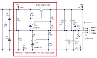
The datasheet of the UCC25800-Q1 proposes the following Postregulator circuit:
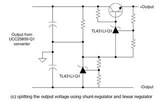

Questions:
a) What are the pros and cons of those different approaches?
b) Is it correct that unbalanced load current is a problem as soon as the difference reaches the maximum TL431 IKA current?
c) How was the circuit on the UCC25800EVM-037 designed? (e.g. Zener voltage of D1 or resistor value of R8 and R5?
d) Is it right that the output capacitors habe to be balanced (matched) to the output voltages for a gate driver supply application? (to have balanced output currents)

Any feedback is highly appreciated.

Thanks and best regards,
Patrick

  • Hi Patrick,

    a) Options for positive and negative rails at the output side:

    1. Single zener diode at one of the rails: low cost, limited in regulation due to tolerances on Zener.

    2. Zener diode and shunt regulator: better regulation for voltage rails, medium cost.

    3. Shunt regulator and linear regulator: best regulation (1% on both voltage rails), expensive.

    b) Balancing the output voltage rails is very important to prevent any regulation problems. The capacitance ratios and rating play an important role here. The output capacitor between (VDD-COM) and (COM-VEE) should be proportional to (COM-VEE) and (VDD-COM) respectively, so the charge is balanced for both caps (Q=C1*V1=C2*V2) and avoid unbalanced current.

    c) UCC25800EVM-037 is designed to achieve 1% regulation, so it uses a shunt regulator and a linear regulator as well.

    d) Yes, output capacitors at the gate driver sides need to be proportional to the respective voltages as explained above to prevent large unbalanced current and variations at the COM pin.

    Thank you.

  • Hi Manuel,

    Thanks for the answers.

    For questions a) and c) I need a more detailed answer. 

    a) The two pictures of my first post show two different circuits. For first sight they look the same but they are not. So my question was why TI did the implementation as shown in the first picture and not the proposed circuit from the datasheet (second picture)? Pros and Cons of this two shown circuits?

    c) This question is related to question a). How are the devices D1, R8 and R5 dimensioned?

    Regards,
    Patrick

  • Hi Patrick, I am taking care of this thread, and I will be back to you soon today.

    Thank you

  • Hi Patrick,

    a) The only difference between both is that D1 is connected in parallel with TL431 to regulate negative voltage rail. This helps to reduce current stress on both devices, preventing saturation and improving regulation accuracy. The drawback is cost.

    c) D1 is a zener diode which is rated for (COM-VEE) voltage. R5 and R8 bias TL431 devices. Depending on (VDD-COM) and (COM-VEE) voltages and current bias of TL431 (check datasheets), R5 and R8 are designed.

    Thank you.

  • Hi Manuel,

    That is only half of the truth. R8 is also a difference. In the first picture R8 is connected to the COM rail. However in the second picture there is a resistor from shunt reference connected to VDD rail. Shunt reference is connected directly between COM and VEE.
    Would be good/helpful  having more information on how the circuit on the UCC25800EVM-037 has been calculated.

    Regards,
    Patrick

  • Hi Patrick. 

    Yes. In the case of the Datasheet, the resistor biasing TL431 is connected to VDD and int he case of the EVM, it is connected to COM. The difference will be the size of the resistor. For the first case, it will be designed with a higher resistance value as (VDD-COM)=23V, and for the second case R8 will be designed with a lower value as (COM-VEE)=5V. Also, the power rating for the first case will be higher. The second case is more convenient as the resistance and power rating are lower. But you can use both methods to bias TL431.

    Thank you.