This thread has been locked.

If you have a related question, please click the "Ask a related question" button in the top right corner. The newly created question will be automatically linked to this question.

UCC256403: Power management forum

Part Number: UCC256403


Hello,

I am developing an LLC supply that goes from battery voltage (~14V) to 500V using the UCC256403. During an inital bring-up, we are able to charge a small capacitor very quickly to this voltage, but when we put our actual load (2000uF), we get less than 100V. A big reason for this is that the supply triggers the ZCS protection on the controller IC. I've tried many combinations on VCR, ISNS, BW, and LL_SS to try to improve this but it continues to happen.

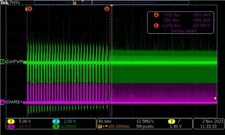
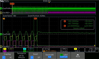
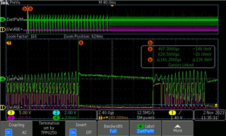
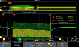
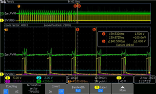
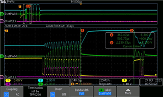
Below is my plot showing that ZCS is detected, then the dead time increases to ~140us. Ye = low-side gate signal. Pu = high side gate signal. Gr = ISNS. Bl = VCR


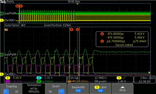
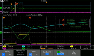
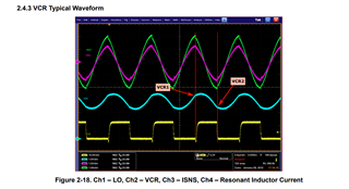
Looking a little closer, I noticed the timing between VCR and ISNS is not correct. Can you comment on this? I included a screenshot from the bring up guide that shows the correct timing for comparison.


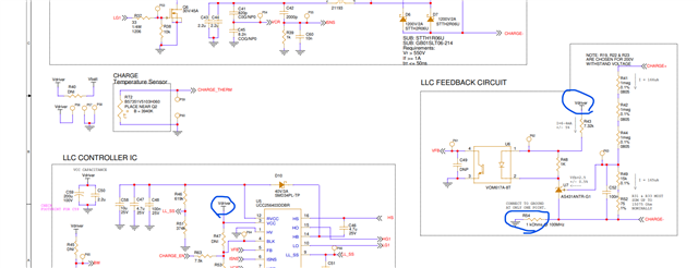
I've also attached my design calculator workbook and SCH if those need to be referenced. I'm curious what the recommendation is to avoid ZCS.

Thank you.

LLC_SUPPLY_WIP.pdfUCC25640x Design Calculator_0v2_working.xlsx

  • Hi Patrick,

    Your post is being reviewed and our expert will get back to you shortly.

    Regards,

    Jonathan Wong

  • Hi Patrick,

    You need to use separate power supply (like a flyback or using aux winding on the same transformer) in order to bias the shunt regulator. You can not use primary side VCC to bias it.

    Regards

    Manikanta P

  • Hi Manikanta, 

    Thanks for the response. I decided not to connect the BW pin to any supply. In my SCH, you can see R45 is not populated. I made this decision based on the Bring Up Guide which lists the following:

    Thanks,

    Pat

  • Hi Pat,

    Sorry about the confusion. I was talking about these connections.

    Regards

    Manikanta P

  • Manikanta, 

    I understand that this is not an ideal setup and something I need to look into but I still don't believe that's my issue. I've tested with a very low output voltage on the shunt (regulating the output to 10V instead of the desired 500V). The FB pin worked well at the smaller output voltage but I continue to see the ZCS kick in and cause 140us between switching. I believe it has something to do with my ISNS values but I can't seem to find a combination that will work for me. I've also tried increasing my BMTH limit to try to keep FBreplica below BMTH for longer to allow the supply to reach steady-state before allowing ZCS to kick in. 

    For reference, my FB pin @ P61 is clamped to 6V throughout operation.

    Thank you,

    Pat

  • Hi Patrick,

    I am not saying that this would cause the ZCS to trigger. I was saying that this is not the ideal way of biasing the shunt regulator.

    Coming to the ZCS issue, could you share the LL/SS pin voltage? This would confirm whether ZCS is keep detected.

    Regards

    Manikanta P

  • Hi Mainkanta,

    Thanks for the feedback. I am attaching several screenshots below. In all of these, Yellow is the low-side gate. Blue is the LL/SS pin. Purple is the high side gate. Green is the ISNS pin.

    The first screenshot (pic 1) shows the first 350ms+ of my capture. About halfway through that capture, the behavior changes so I'll show you both sides.

    Here's a close up of one of the pulses during the first half (pic 2) and zoomed-in photo (pic 3) of the switching frequency (150kHz) of the pulses in the first set of pulses on the left.

    From pic 3, I used cursors to display the values on ISNS (pic 4) followed by the 140us blanking time (pic 5) that I believe is due to ZCS but happy to hear other suggestions.


    Here is a screenshot (pic 5) of the longer set of pulses at the end of the waveform from pic 2. Here, switching occurs fine until I lose VCC after 1ms due to being on a current-limited supply that cannot supply the necessary current for the voltage to stay above the UVLO limit of the controller. 

    From pic 5, I captured the switching frequency (133kHz) in the below screenshot (pic 6)


    The last two screenshots are from the right-hand side of pic 1. The first (pic 7) is a zoomed-out screenshot and the second (pic 8) is zoomed-in and also displays the 140us blanking period.


    Thanks for taking a look at this. I've tried many combinations around the LL/SS pin, ISNS pin, and the Vcr pin, but I'm open to hearing more suggestions as I haven't been able to get the supply to work properly.

    Best,

    Pat

  • Hi Pat,

    Thanks for sharing the screen shots.

    I have looked at your design calculator again to see the tank is designed properly.

    The maximum gain requirement is not able to meet by the current design which is shown below.

    You will have to modify the tank parameters such that max gain requirement is met. I would also strongly recommend using the simplis simulation before you implement the design in hardware.

    Also, reduce the ISNS cap value (C60). 10nF would cause more phase difference compared to actual resonant current phase which would cause faulty ZCS triggering.

    Regards

    Manikanta P

  • Hi Manikanta,

    Thanks for the feedback here - I removed C60 and was able to avoid the ZCS caused by the phase shift. I wasn't able to unlock the Design Calculator so I couldn't expand the graph to view what you took a screenshot of, but I am reviewing the design now too. 

    Thanks for your help on this.