This thread has been locked.

If you have a related question, please click the "Ask a related question" button in the top right corner. The newly created question will be automatically linked to this question.

TPSM63603: sch review

Genius 3870 points
Part Number: TPSM63603

Hi there

we are using this device. some questions to ask.

1. Is there internal pull-down resistor on EN pin?  what is the device status if the input EN is Un-connected(floated) by mistake?

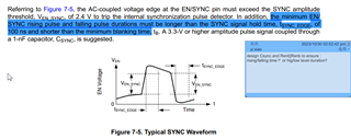
2. we use external sync to multiple TPSM63603. Section 7.3.7 mentions (blue high-lighted) that "the minimum EN/SYNC rising pulse and falling pulse durations must be longer than the SYNC signal hold time, tSYNC_EDGE , of 100 ns and shorter than the minimum blanking time, tB(4us, min).

here is my confusion: Does the "EN/SYNC rising pulse and falling pulse durations " refer to the rising/falling time (say, from 10% to 90% generally), or refer to the high / low level duration? I think it is the latter。

3. can we connect small SMT test point on SW pin, as we hope to measure switching node waveform.

4. could you please help review our desing sch. 

we use 800khz ext. sync, and two IC can be enabled sequentially by connecting PG of U1 to EN of U2 (R1617), and also can be enabled at the same time by sharing net "PWR_EN2_share"(R1712)

[deleted]


thanks a lot!

  • Hi Yi,

    1. No, with the EN pin floating, there is no guarantee that the device will power on or operate as expected. If the EN/SYNC pin is below 0.4V, the device will be in shutdown mode (internal LDO and regulator both disabled). If this pin is between 1.1V and 1.263V (typ), the device will be in standby mode (internal LDO enabled, regulator disabled). For the device to regulate properly, the output of the internal LDO (VCC) must be above its UVLO threshold and the EN/SYNC pin must be above the precision enable threshold. See section 7.4 in the datasheet for more information on device functional modes. 

    2. Correct, this refers to the high/low level duration.

    3. Yes, a small SMT test point can be used to monitor SW. As mentioned in your screenshot, the test point can introduce more noise and EMI emissions. If this is not a big concern, there should be little effect on the device's ability to switch and regulate. 

    4. Overall, the schematic looks good! Is there any intention to populate the NC components? Also, can I ask what the purpose of the enable circuitry on the first device is (as opposed to just connecting EN to VIN directly)? 

    Let us know if you have any additional questions!

    Regards,
    Carol