This thread has been locked.

If you have a related question, please click the "Ask a related question" button in the top right corner. The newly created question will be automatically linked to this question.

LM5050MK-1EVAL: Oring SCH review

Part Number: LM5050MK-1EVAL
Other Parts Discussed in Thread: LM5050-1

Hi team:

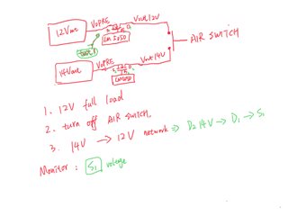
 My customer use LM5050 for the function of preventing backflow. Would you help to review the SCH and issue?

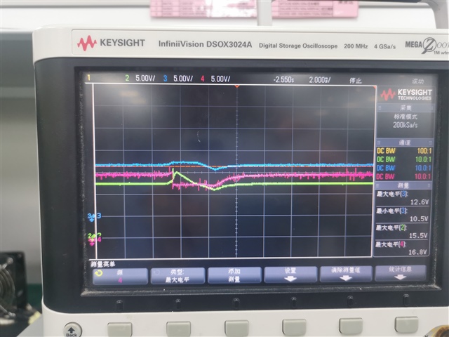
 The current phenomenon of the product is that if the output has no load and light load. The backflow function works here . The waveform attached as below:

 Green is VOUT(6PIN)

 Blue is VOPRE(4PIN)

 Red is the driver of lm5050(5pin).

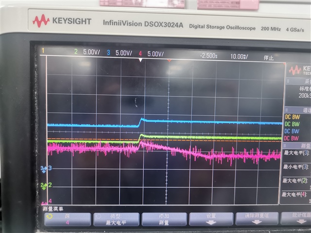
But when the product is fully loaded and the output current is increased, The backflow function not works here .  The waveform attached as below:
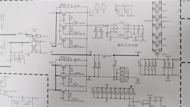
SCH:

  • Hi Allen,

    Thanks for reaching out to us. Let me check and get back to you within couple of days. 

  • Hi Allen,

    Can you explain the test conditions in the waveforms shared and what you think is the unexpected behavior.

    Also in the schematics, what are the FETs being driven by the controller gate, OR_G rail ? I do not see them in the schematics. 

  • hi Praveen:

     I write a note for reference in this case.


    1.The outputs of the two prototypes are connected in parallel, and a air switch is used for isolation in the middle. One is 12v, and the other is 14v. The 12v prototype first outputs at full load, then closes the air switch, and connects the 14v voltage to the 12v prototype. The oscilloscope measures the output isolation respectively. The voltages at the D and S terminals of the mos were found to be raised to 14v.

     and this mean it cannot prevent backflow, we monitor the S1 voltage of the mos. If the voltage is raised, it means it has failed. Just like this picture above, blue is the voltage at the D1 of the mos  , green is the S1 voltage, and the S1 voltage has obviously been raised.

    2.The driving pins of the IC are connected, maybe the schematic diagram cannot be seen clearly.

    3.The rise time of the reverse voltage is about 10ms.

  • Hi Allen,

    Thanks for reaching out to us. Today is a Holiday in TI India, let me get back to you within couple of days.

  • Hi Allen,

    Thanks for the explanation. 

    In the waveform below, when Vout rises to 14V, the input can be seen rising to 14V as well. This can generally happen when

    1. The reverse current flow from Vout to Vin is less than the VSD(REV)/Rds(on) threshold which is required for the gate to turn OFF immediately
      1. In this case as there are multiple FETs in parallel, the amount of reverse current (= VSD(REV)/Rds(on)) required to turn OFF the gate immediately is very high. 
    2. You are testing with a input power supply (like DC-DC buck converter) at 12V rail which cannot sink negative current. In this case a small reverse current is sufficient to pull the 12V rail input to 14V as this node cannot sink in current. 
      1. If you measure the reverse current flowing from Vout to Vin, you will see there is no reverse current flow.


    The gate can be seen slowly falling which is due to the linear gate control of LM5050-1. For more understanding on this topic, please refer to section ‘6.1 Linear Regulation Control Vs Hysteretic ON/OFF Control’ of Basics of Ideal Diodes  Application note.