This thread has been locked.

If you have a related question, please click the "Ask a related question" button in the top right corner. The newly created question will be automatically linked to this question.

UCC21225A: UCC21225A OUTA pin output abnormality

Part Number: UCC21225A

Hi,

The voltage of the VCCI pin of UCC21225A is 9.5V, the voltage of the VDDA and VDDB pins is 11.2V, the Disable pin is connected to the ground, and the INTA and INTB pins provide input signals. The OUTA output is abnormal (no signal output), and the OUTB signal output is normal. Please help analyze the cause. The schematic diagram is as follows:
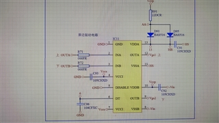
Thanks!

  • Hi Jeno,

    For your deadtime configuration, are you trying to disable the deadtime? If so, the effective way to disable the deadtime would be to tie the DT pin to VCCI. This will allow the outputs to completely match the inputs.

    If a specified deadtime is desired, there must be a programming resistor to set the appropriate deadtime value. Refer to section 8.4.2.2 of the datasheet.

    Hope this was helpful!

    Best regards,

    Hiroki