This thread has been locked.

If you have a related question, please click the "Ask a related question" button in the top right corner. The newly created question will be automatically linked to this question.

PMP41009: UCC28740-Q1

Part Number: PMP41009

Hi:

I have a question about the selection of Rcs and Lp.

In my design, the Lp calculated by sluc487b is too large. This will make the volume of the transformer large.  If I choose a smaller Rcs I can reduce the value of Lp.

So I want to know what the shortcoming of this is? Will increase the peak current of the primary side? making the duty cycle very low? making the output ripple increase? and are there any other problems?

How should I make a choice?

Thank you very much, You've helped me a lot.

  • Hi there,

    I have contacted the designer to have her help on the questions here. She should be able to reply shortly.

  • Hi, 

    As you said, a smaller Rcs will increase the primary peak current, you need more turns for the primary side of the transformer to ensure it wouldn't be saturation with the peak current. And it also increases the output over current point.

  • Thank you Sheng-yang

  • ok thank you,I need some time to understand what you're saying. And I have another question about PMP41009.

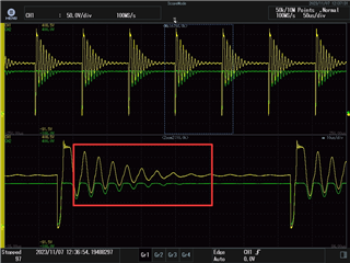
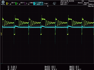
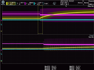
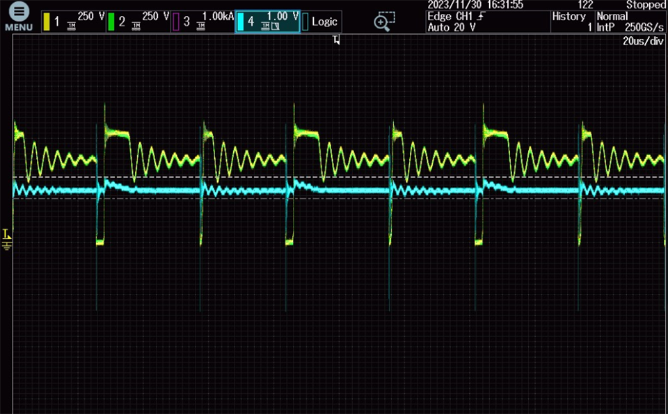
    This figure is upper FET Drain to GND voltage(CH1) and lower FET VDS(CH2)。

    As shown in the red rectangle, the primary side occured a large oscillation. How can I improve this waveform?

    Thanks again.

    Best wishes for you!

  • It is normal operation waveform, you needn't to improve it.

  • okey, Thank you very muck

  • Hi Linda,I was faced with a new problem:

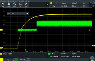
    I put an electronic load on both ends of the output, and when the constant current output mode is used, if the current is close to the designed maximum output current, the circuit will not start. But it works in constant resistance mode。

    What are the possible reasons for this?

  • You can check if the CC mode output current has a spike. What's the output voltage on point (带载点)? You can also increase it and redo the test.

  • The designed output power is 2W and the output voltage is 15V。When the electronic load‘s CC mode current is 0.06 A ,it can work.but can not work in 0.08A.

  • And I do not understand what means "output voltage on point", Is it the time to connect the load?

  • Yes, it is the output voltage at the load on point. From the waveform it seems that you set it to 0V, could you increase it? Acutely a 15V end equipment won't start up at 0V.

  • I changed the output voltage at the load on point,But these problems remain.

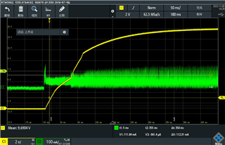
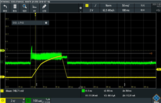
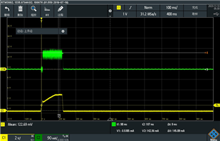
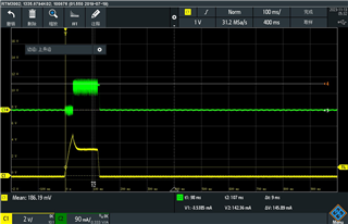
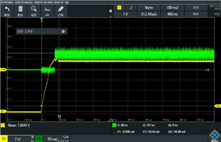
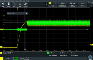
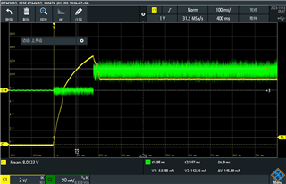
    These pictures show the power-up process at different load on points

    2V:

    5V:

    10V:

    12V:

    13V:

    14V:

    Adding a load too early will cause the output voltage to drop to zero, Or stabilize to an unexpected voltage。

    I wonder what happents in this prosess. Can you help me analyze it?

    Thank you very much!!

  • It should go to the constant-current (CC) regulation. You can try to add a 100pF capacitor from CS to GND, if no improvement, you should increase the target output current in constant-current regulation.

  • I tried adding a 100pF capacitor from CS to GND as you said but it didn't work.

    And now I find that the load capacity of the output decreases with the increase of the input voltage. For example, with the same resistance load, 580V input can output 15V 5.6W, but when the bus voltage rises to 800V, the output becomes 9.5V 2.24W.

    According to my observation, the duty cycle of the switch is always very low, is this the depth DCM operation mentioned in the excel table?

    Is the duty cycle causing the load reduction problem?

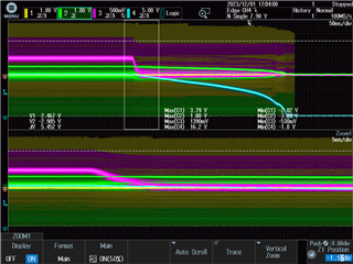
    When the load is increased, the FB pin potential changes from about 1V to about 0V. What may be the cause of this?

    CH1:VCS,CH2:VVS,CH3:VFB,CH4:Vout

    Thank you Linda.

    Need your help q(≧▽≦q)

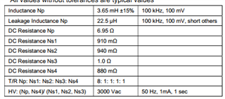
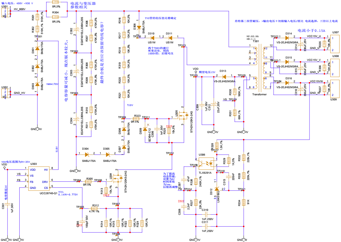
  • Please share the schematic and the transformer spec with me.

  • this is the  schematic and the transformer spec

  • A little different between the actual PCB and schematic that the gate resistance of the two MOSFETs is 1Ω, and the C313 is 150 NF.

  • Some of the problems I have observed so far are as follows:

    1. The duty cycle is always very low, and the Dmax calculated by the excel table is less than 0.131.

    2. After loading, the VDD voltage increases significantly(up to 27V、28V), why can it continue to work without triggering output overvoltage protection?

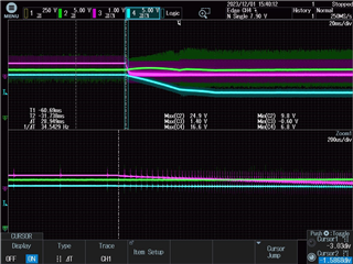
    3. As mentioned earlier, at the moment of output loading, FB voltage drops to around 0V, and VDD voltage begins to drop. However, I tested the FB voltage when the bus voltage was 400V, and the FB voltage only dropped to about 0.6V at the moment of loading while the VDD voltage remained stable. Is this due to loop instability?

    waveforms at 400V input(CH1:VDD,CH3:FB,CH4:Vout)

    waveforms at 600V input(CH2:VDD,CH3:FB,CH4:Vout)

  • 1. The transformer turn radio is low, so the duty cycle is low, you can increase the turn radio to increase the duty cycle.

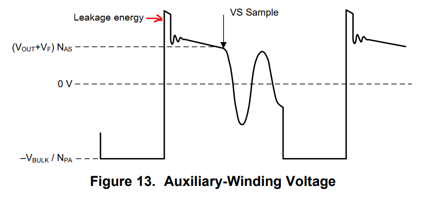
    2. VDD rises to 27V due to the leakage energy delivery to the VDD capacitor during high load conditions.so the VDD voltage increases with the load. The output voltage discriminator blocks the leakage-inductance reset and ringing while continuously sampling the auxiliary voltage during the down slope after the ringing diminishes. so it will not trigger the output over voltage protection.

    3. From this waveform, we can see the duty cycle isn't constant, the control loop should be instability, you can try to change the FB resistors and capacitors and the secondary compensation components to be same as PMP41009.

    4. Change R312 to 1.5k, populate C305.

  • Thanks for your reply.

    And i wana know that dose the low duty ratio affect the stability of the control loop?

    Can The resistances and capacitors  be set the same as PMP41009 while I used a different optocoupler and adjustable shunt regulator than PMP41009?