This thread has been locked.

If you have a related question, please click the "Ask a related question" button in the top right corner. The newly created question will be automatically linked to this question.

UCC28951: When stepping the reference from 0, there is a delay until the converter starts switching.

Part Number: UCC28951

I have a converter design utilising the UCC28951, acting as a current generator. There is (almost) no output capacitance.

The internal error amplifier is bypassed by shorting the EA- and comp legs and an external current regulator measures the output current, adjusting the reference to EA+ accordingly. The converter operates in Peak Current Mode

The switching frequency is 50kHz.

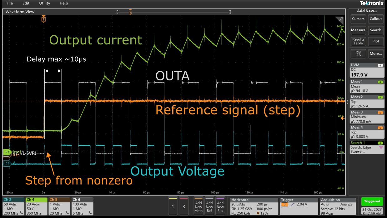
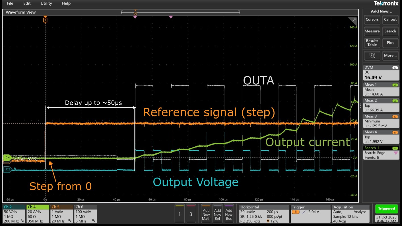
The problem arises when increasing the input reference (EA+) from below the switching threshold(~0.8V) to a higher value. This results in a delay of approximately 50µs before the converter begins switching, which is not suitable for the intended application. This can be seen in the following image:

However, when the reference step is initiated from a higher level where the converter is already in operation, there is no noticeable delay.

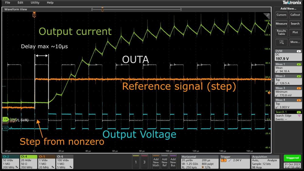
I suspect that this issue may be related to the burst mode function of the converter. It's possible that the converter initiates in burst mode when starting from zero and takes some time to transition out of this mode. This might be a wrong assumption.

I attempted to address the problem by setting the Tmin resistor to its minimum value of 10kΩ, but this adjustment did not resolve the issue.

Question: Is there a way to remove this initial delay when stepping from zero?

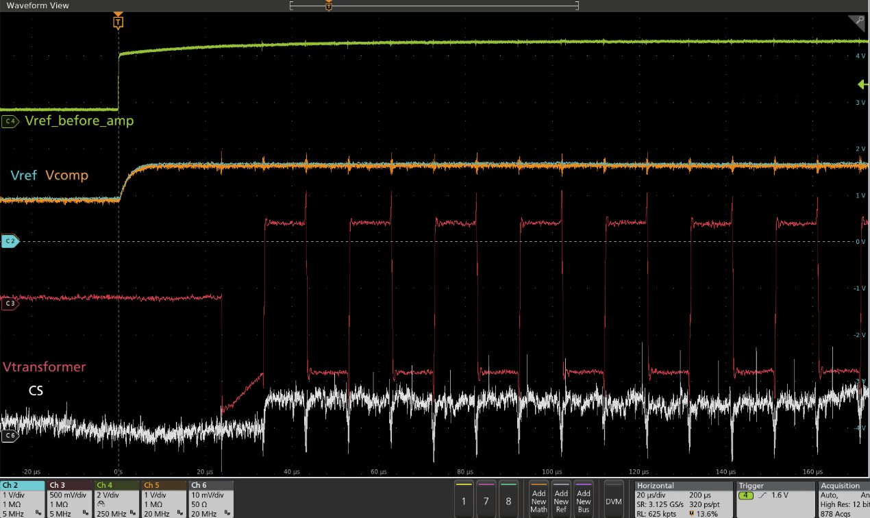
Note: An amplifier circuit is positioned between the reference signal depicted in the plots and the EA+ leg of the controller. Its purpose is to ensure the appropriate scaling of the reference signal (from 0.8V to 2.8V). It's important to note that this circuit operates correctly and is not the source of the issue.

  • Hello,

    I am reviewing your inquiry and will get back to you shortly.

    Regards,

  • Hello,

    I wonder if this delay could be do to soft start.  Could you retake these with the soft start (SS) pin voltage to check?

    Regards,  

  • Hey Mike, thanks for the response.

    I've repeated the measurements, this time looking at the SS pin(red line) simultaneously. I'm not running power through the system, but the same issue as before can be seen when looking at the Gate signal A.

    It does not seem like this has anything to do with the SS voltage, since it is at a constant voltage.

  • Hello,

    I am reviewing your inquiry and will get back to you shortly.

    Regards,

  • Hello,

    From these plots I cannot see where the SS pin ground is referenced.  Could you tell me where the ground reference for all channels?

    Also the bottom plot seems to have switching before the EA+ and reference come up.  This is strange.

    Is your reference voltage the device reference?

    Regards,

  • Hey

    All the signals except the orange reference signal are referenced to the same ground level. They are y-axis shifted to allow for a better overview, but Ch6 and Ch3 ground are referenced by the red flag on the left hand side. Ch1 and Ch5 are referenced by the yellow flag on the left hand side. 

    SS has a constant voltage of around 4.7V

    As i attempted to explain earlier, the "reference signal" is what I'm feeding as a reference to the converter. This goes through an amplifier circuit, which adds an offset and a gain. The converter has an internal PWM comparator comparing the EA+ signal to a ramp going from 0.8V to 2.8V. Therefore, the converter should only start switching once EA+ hits 0.8V.

    In the bottom plot, there is switching before stepping. This is intended, as to show a step from above 0.8V on EA+, to a higher voltage. The upper plot shows a step from below 0.8V on EA+ to a higher voltage.

    So what I'm seeing, is if I perform the step from no switching -> switching, I see a delay.

    If I step from switching -> switching, there is no delay.

    Hope that clears things up.

  • Hello,

    I am reviewing your inquiry and will get back to you shortly.

    Regards,

  • Hello,

    Thankyou for the clarification it is appreciated.

    So from the waveforms the SS is completed and is steady state.  So the device is not soft starting and does not look to be going into over current hiccup mode.

    This previous waveform as actually your output is sliver pulsed or a minimum duty cycle.  The output voltage is mostly like the voltage across the output inductor and output ground.  After looking at this waveform, I believe that you might be hitting the cycle by cycle peak current limit when you introduce the reference voltage. 

    You should study the CS pin, voltage amplifier output, Out A, Out B, reference and EA+ when you apply the output voltage.  This will help you understand why the duty cycle is terminating earlier than it should. 

    Regards,

  • Hello Mike, thanks for your answer. I am still however working on this issue.

    I should make it clear, that this converter operates as a current generator, with no output capacitance. 


    The problem is still that there is a difference in how quickly the converter reacts to a step reference when starting from zero, compared to starting from a non-zero reference. The question regards the load step response delay of UCC28951. The response time when stepping from no load reference to full load differs significantly from stepping from low load to full load in our measurements. 

    I have measured the CS signal, and this is not the issue. There is no signal on the CS pin, since no current is flowing.

    A step response from low load only has a delay of half switching period, while when stepping from no load it has a delay of 2-3 switching periods. For our use case for this controller, this is unsatisfactory. We need to get the delay in the load step response from no load down to max 1 switching period.

    The converter is operating at steady state before the load step, so the soft start capacitor is fully charged. The DCM pin has been shorted to ground. RTmin is set to the minimum allowed 10 kOhm, giving a Tmin of 59.2ns and a minimum duty cycle of 0.592% for the 100 kHz oscillator frequency used in this design, in accordance with the datasheet.

    At no load the reference duty cycle is 0. Is there some sort of hysteresis built into the controller when going out of shut down mode?

    Could we perhaps increase the oscillator switching frequency during no load to increase the response time?

  • Hello,

    I think when you are at no load the comp output will go as low as it can.  When you demand a load the comp starts from a zero condition and will have to climb to a voltage where the converter is demanding a duty cycle greater than the minimum on time programed by Rtmin.  You should be able to verify this by looking at COMP, CS and the input of the transformer.

    1.  I would test it with light load to full load where you mentioned there are no issues.

    2.  Then test from no load to load where you see the issues.

    3. When you compare the two test conditions it will come apparent.

    If you need a fast transient you may be able to pre-load the output to ensure a minimum duty cycle is maintained under no load.  So that when you converter demands greater load there will be no delay.

    Regards, 

  • Hey Mike.

    I've made some measurements, looking at the comp signal compared to the EA+ signal reference into the controller. Sadly, this has not made my understanding much better.

    Step from 0:

    Step from load:

    It will perhaps be necessary to have the converter always output some signal, such that it never goes to the no load state.

  • Hello,

    I am evaluating your inquiry and will get back to you shortly.

    Regards,

  • Hello,

    I believe my previous explanation that was causing the delay was correct, even though the waveforms are not showing it.

    One thing that is confusing about these waveforms is when VREF before the amplifier comes up on the top waveform there is no voltage applied across the transformer and the comp has 1 V on the output.

    On the second waveform the comp is at 1  V with partial load and has minimum duty cycle and input voltage applied across the transformer.  

    The comp voltage should be at 2 different voltage levels when there is no load and partial load.  At no load the comp output should be much lower than it was with partial a load.  

    Could you double check these waveforms?  I would expect the comp to be below 0.8 V under no load conditions.

    Regards,