This thread has been locked.

If you have a related question, please click the "Ask a related question" button in the top right corner. The newly created question will be automatically linked to this question.

LM2717-ADJ: 2 of 5 worked, others just heat

Part Number: LM2717-ADJ
Other Parts Discussed in Thread: LM2717

schematic_power_section.pdf

Hi,

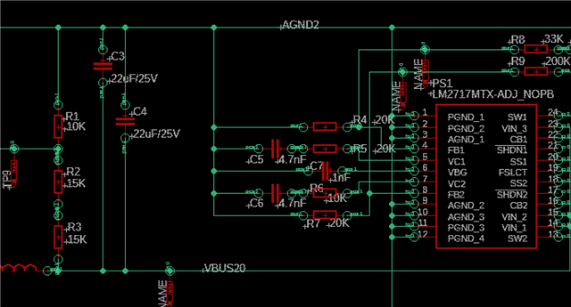
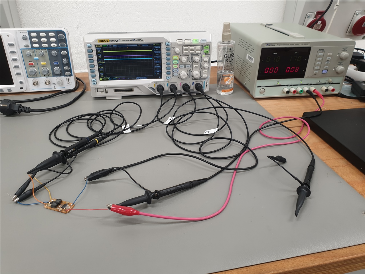
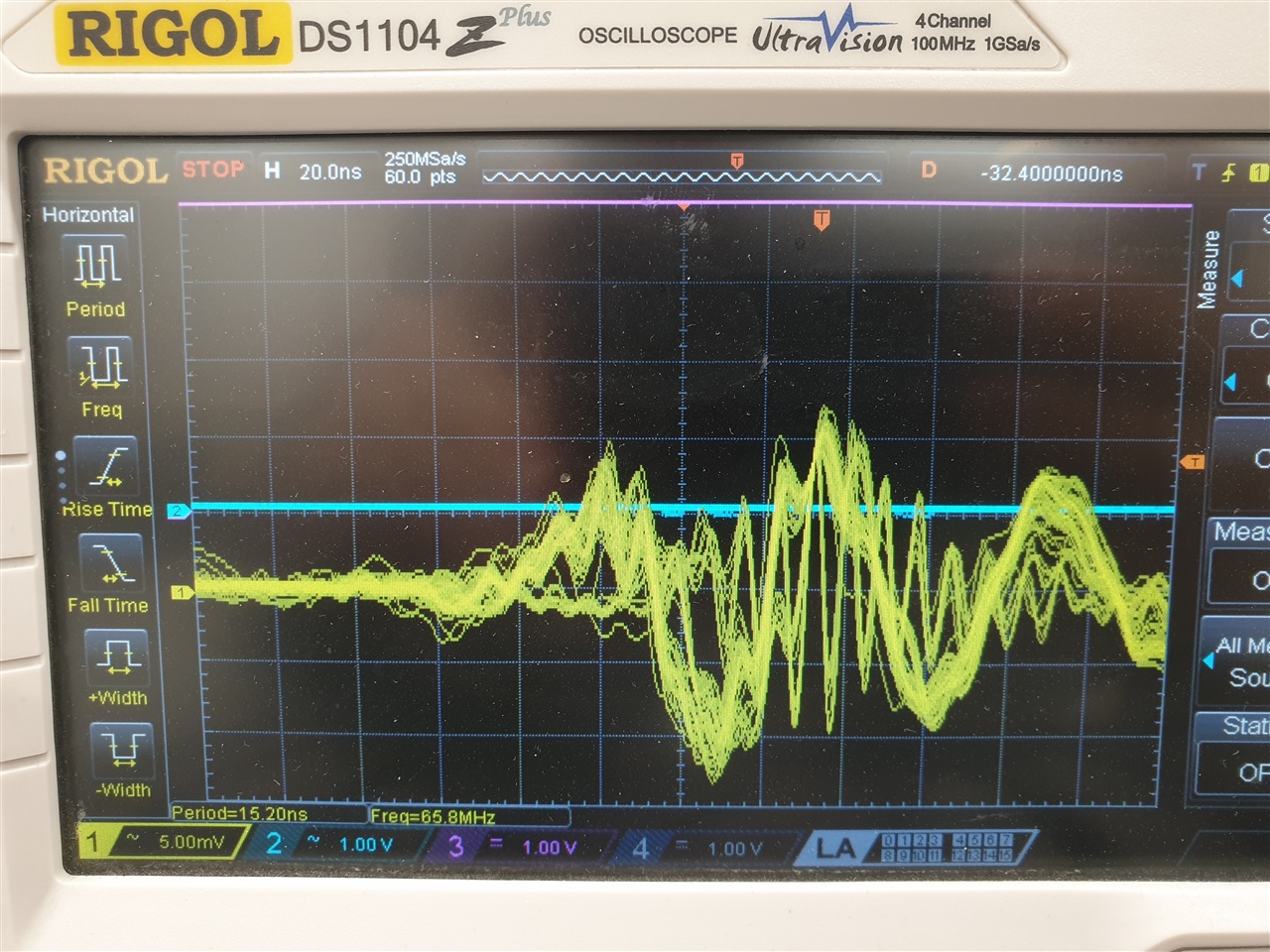
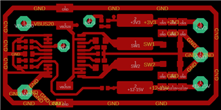
thats the schematic I have, but the device doesnt work.

I have bought 5 of LM2717ADJ, but only 2 of them worked, I dont know where is the problem,

because the schematic is just from typical aplication note in datasheet.

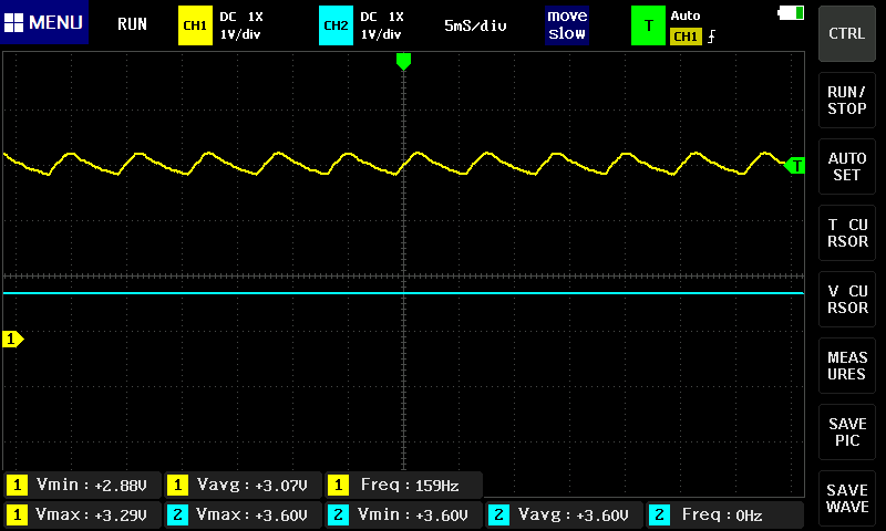
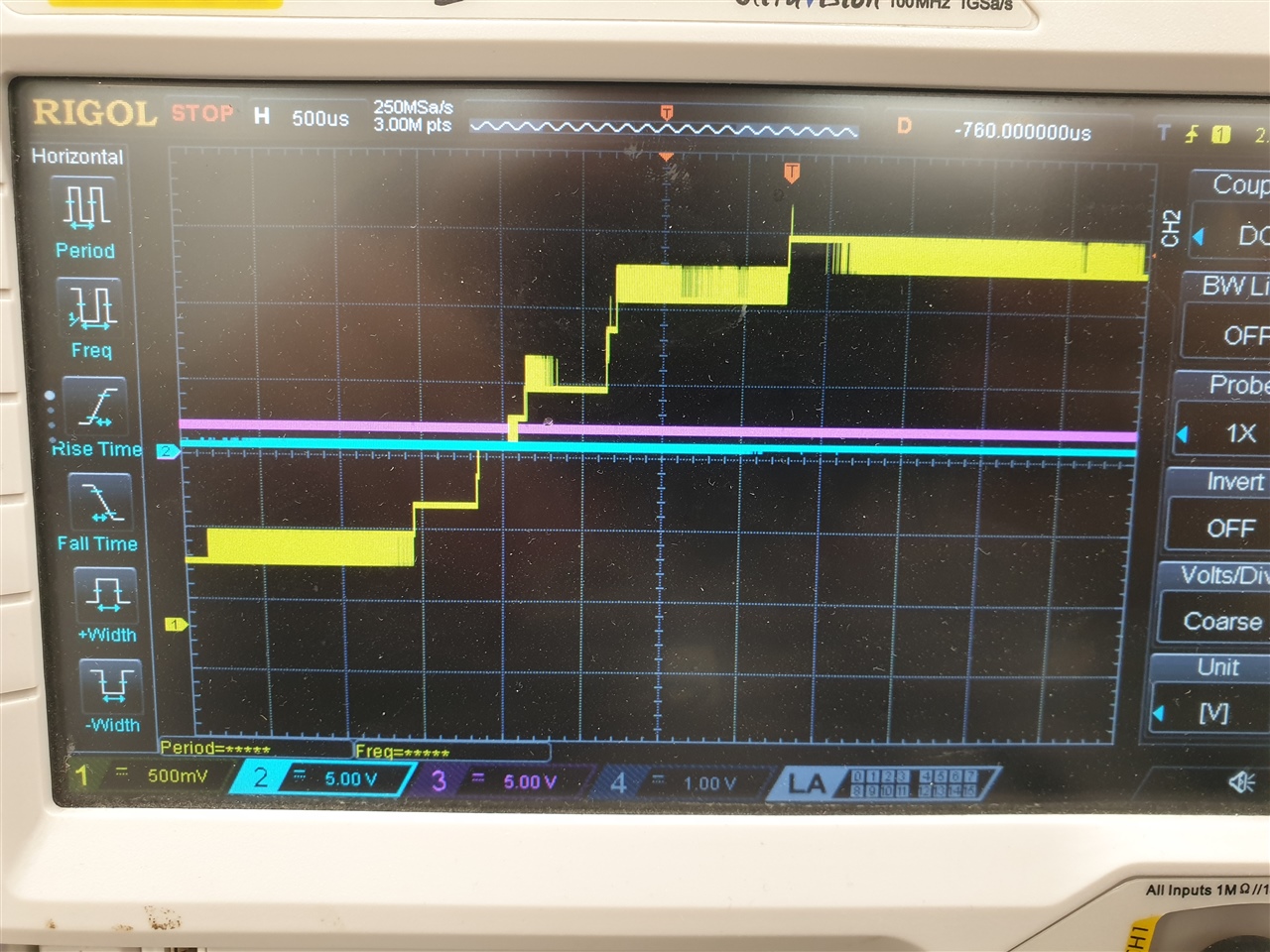
Some of bad ones were heating but I think one of them was just doing nothing. 

The voltage on input was 18.53V and I wanted 3.3V and cca 12V on the outputs.

I know, there was mistake with resistor dividers,(I just mis-read thing about internal divider) - its feedback (this couldnt destroy IC, even though, the calculated voltage would be around 3V... )

At least, there are two buck converters, and the mistake was only on the first, second divider was good.

I changed the wrong divider later but anything changed.

Could you please review the schematic and tell me what could possibly cause damage?

Or, at all... whats wrong?

Thank you very much

  • Hi Ondrej,

    More critical problem in your schematic is that No Cin is placed for part. It could cause converter unable to startup. Please add Cin based on recommendations on ds and have test for your parts to see whether they could work normally.

    BRs

    Zixu

  • Hi Zixu,

    Im sorry for this, the scematic it self is a part from bigger shematic for my board, as a Cin I have 2x 22uF/25V which are on the same board on VBUS20 line

    as in this image:


    Kind regards

    Ondra

  • Hi Ondrej

    My colleague will check it and give you a feedback early tomorrow, thanks!

  • Hi Ondrej,

    Schematic looks good from my side. Could you please help to share layout? And could you please help to check whether All LM2717 are soldered well on your board?

    For your mentioned "heating", Does chip have dramatic temperature rise? what about loading for the heating parts? What about phenomenon about other bad parts?

    Could you please help to capture waveform of Vin, Vout, SW, IL as well?

    BRs

    Zixu

  • Hi Zixu,

    I can share layout, Im 100% sure that all LM2717 were soldered properly, I soldered them one by one with different techniques, such as hot air, pin by pin as short as possible and even with IR heater + hot air at final temperature rise. I have done all what I could I believe.

    Heating was wery significant, I couldnt handle finger on it in few seconds, also IC which is powering all this dropped the voltage down as it was overloaded.

    these parts had no load, just the capacitors for futher powersupply. These are not shorted.

    I can give you waveform on the input, but at the output was zero... so there for I cant measure waveform.

    Over the weekend, I made my self another PCB and tested every of those LM2717
    there is the layout, I wanna say, it was made in order to check the functionality, it is as simple as possible and I made it with my hands lets say, it is not by PCB manufacturer, which made the first pcb (where were the ICs just heating)

    One of the ICs I tested over the weekend, was kind a working, on the output was 3.3V and 7V. The IC was heating but not much..

    Under even very light load it gave ouput to zero and if I unplug the load, it has had some output, but lower then previously.

    It was powered by very powerfull DCDC converter with bug enough capacitors (I limited current to 3amps at 17V)

    so the input for LM2717 we can consider as very stable (I checked it with osciloscope but dont have images)

    I dont understand this behaviour...

    Here is the layout and schematic (check the values - little changes) of my test board:

    4478.schematic.pdf    Im sorry for value placement in schematic....

  • Hi Ondrej,

    I will check the layout and wait for your waveforms!

    BRs

    Zixu

  • Hi Zixu,
    Please, can you specify more the waveforms you want?

    I mean, on ouputs was zero.. so dont want its waveform.
    Input was very stable the Voltage diference was +- 10mV. Very stable I think

    Here Im sending you the original layout on my board:


    Output capacitors are on the other side of the board, directly under the coils.

    BRs

    Ondra

  • Hi Ondrej,

    Zixu is checking and will reply you soon.

  • Hi Ondrej,

    I just want to check waveforms to understand the current condition of converter, so Vin+Vout+SW+IL(inductor cuurent) are needed. Vin is captured to determine whether the VIn of converter exceeds its UVLO threshold. SW is captured to check whether it start switching. Inductor current is captured whether there would be some over-current conditions. Vout is captured to check the final results for voltage converter.

    And please help to capture waveforms both in startup period and steady state.

    BRs

    Zixu 

  • Hi Zixu,

    I understand, but I have only 2 channel oscilloscope, and more about it - the channels are not isolated between each other.

    At least I tried to capture something and this is the 3V3 output under very light load (cca 82R) (Yellow color)
    The blue one is another output (where I wanted 12-15V)

    The second output was not switching, it was acting just as a resistor divider, when I gave some light load there, the voltage dropped to zero, when I disconnected the load, voltage came back, but to lower value, than previously.


    BRs

    Ondra

  • Hi Ondrej,

    If converter stops switching, there would be no output for shown channel. Supposing there would be switching pulse but needed to be shown. Waiting for your waveform.

    BRs

    Zixu

  • Hi Zixu,

    You are right, thats normal behaviour of nearly every dc converter with overcurrent protection, but this one even didnt started switching.

    It was just heating but power mosfet was not switching, because otput was just zero..

    Basically the ouput of the converter was just heat.

    Now Im not able to measure any other waveform, because I gave it to my friend, also enginneer, so he will try to find out some way to power it up, and maybe he will find some solution.

    As far as I tested,  the converter was not starting, as soon as I powered up the original board, the converter which was supposed to power this converter, just came down (in some cases) to around 4V because of overload.

    I really dont see the reason why the chip should not start up normally...


    BRs

    Ondra

  • Hi Ondrej,

    Understand your conditions. But for abnormal part,  first we need to check whether EN and Vin reach rising threshold to check whether chip could start, second we need to know SW+IL waveform to check whether there would be some abnormal operation instead of just having description of heating and non-switching. Waiting for your waveform.

    Supposing the part triggers OCP since the Vout is quite low and chip could not output big current.

    BRs

    Zixu

  • Hi Zixu,

    I understand, so I will try to measure everything you wrote over weekend, and on 27.11. I will have time for it, I mean, I will be online and
    (if my friend gave me back the board) i will have it on bench with oscilloscope connected. I will definitelly send some waveforms over weekend.
    Thank you for your time even here in chat in order to solve this..

    BRs

    Ondra

  • Hi Ondrej,

    Thanks for understanding! Waiting for your waveform.

    BRs

    Zixu

  • Hi Zixu,

    I didnt expact that, but I was able to test the board out today.

    Im quite sad about the results, because this was the last LM2717adj   which I had not used before and it still behave the same as the others.

    Here are some photos:

    After first power up, where I set trigger to one of the outputs, than the ic heated, i turned it off and second power cycle it was zero on output.

    the last waveform is maybe just a noise.. as u see it is 5mV resolution..

    As I told you earlier, this was the test board which I made just for this IC.

    Thank you for helping me

    Have a nice weekend

    BRs

    Ondra

  • Hello Ondra,

    Zixu will check your waveforms and reply you soon.

  • Long time no activity, I will close this thread.

    If you have further questions, please reply and this thread will be re-opened.

  • Hi Miranda,
    Im still waiting for Zixu's response to the waveforms I send earlier..

    Can you please tell him? He has maybe a lot of work and simply missed this to respond..

    Thank you
    Ondra

  • Hi Ondra,

    Sure, I will remind Zixu to check your waveforms.

  • Hi Ondrej,

    Sorry for late response. Here is my comment:

    1. I have checked layout and find the layout is not good. Supposing layout is critical in this issue. Could you please help to share your full layout?

    2. Could you please confirm Vin is lower than Abs value of LM2717? 

    3. Is 3.3Vout rail able to output big current?

    3. I could only get description not required waveforms for this issue. At present the show waveform could not be able to be analyzed. Since at present 12Vout is abnormal, Could you please help to capture Vin+SW2+IL2+Vout2? 

    BRs

    Zixu

  • Hi Zixu,
    1) Here is an image of the test layou which didnt work either:  (even with the last fresh new chip)

    2) Absolutely, I can confirm that the Vin was way lower than Vmax for LM2717
    3) No, you see in waveform, that was the initial start-up first power-up of the chip ever (after testing in manufacture)..   Than it died as the chips before
    4) Well, I know you want all the values in waveforms but I have only 2 channel oscilloscope (the upper images are from friendly company with 4ch oscilloscope), anyway, there is nothing to measure, the voltage went up in weird "pattern" as you ca see on osciloscope. Then it started heating and died, so it is unreal to capture more waveforms.

    According to this, I gave this chip away and found another, suitable for my needs. 
    I think, its logical Im not going to buy this chip anymore, isnt it?
    The chip died, even if I tried to capture something on VSW legs of chip directly, there was zero under oscilloscope.

    I will use different chip which I already tested and it works (to be precise, I will use two bucks insteda of one chip with two bucks inside)

    The only thing is, because I bought 5 of those, I only want moneay back, because these didnt work.

    Even the time there cost me more than value of the chips.. You know, I just wanted to know if i made a mistake or what, but as far as I see, I didnt, Maybe layout is not ideal, nothing is ideal... But other enginners told me that the layout is good enough for test purposes, in other words, it should work).

    Im giving there all the schematic file and layout file for you, so you can check it.

    I appriciate your time but I dont want to spend more time on this chip.  
    Please tell me what should I say to Mouser, my chip supplier and thats all I think since I dont have any more chips to measure what you wanted.

    LM2717_TEST_Sch.schLM2717_TEST_Sch.brd

    Thank you Zixu,

    and I wish you Merry Christmas!


    Ondra

  • Hi Ondrej,

    I have checked your layout, finding the issue may lie on improper layout shown in following tips:

    1. Cin should be put as close as possible to Vin pin and PGND pin. Current layout has long GND trace from Cin GND pad to LM2717 PGND pin, which could highly trigger issue of unable to startup.

    2. The FB point is not selected well, which is linked to inductor terminal. This could have noise coupled into FB pin and make chip in abnormal operation.


    3. It is recommended to use polygon plane for GND connection instead of using traces. Long traces could have noise as well, which could make chip in abnormal operation.

    4. Components of FB, SS, Vc1 and Vc2, VBG,FSLCT should be connected to AGND, then AGND should be connected to PGND with single point. The layout does not follow this rule well, especially for VBG pin, which provides steady reference for internal control circuit.

    Above layout problems could result in issue shown in LM2717. I would suggest to modify your board or have newly designed layout to try fixing your issue. For check whether chip is damaged, please use diode scale in digital multimeter: positive connect GND, negative test each pin to check whether ESD diode exists for each pin (except SW pins). If ESD diode is not broken, the chip is not damaged with high possibility.

    Since your Vin is less than Abs_max value, I suppose LM2717 is not damaged and could be used once layout is modified.

    BRs

    Zixu