A related question is a question created from another question. When the related question is created, it will be automatically linked to the original question.
If you have a related question, please click the "Ask a related question" button in the top right corner. The newly created question will be automatically linked to this question.
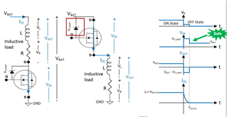
TPS2HB16-Q1: Like this picture. We use a high-side switch to disconnect the inductive load. Why is the VDS=Vclamp when the high-side switch is off?
1. When an inductive load turns off, the inductor will try to maintain the current flow through itself by using all the stored inductive energy. This will cause a large negative spike in voltage on the output. Therefore, the goal of the clamp is to hold the voltage to a value that is acceptable and help dissipate the inductive energy. Therefore, the clamp will activate when the voltage difference between the drain and the source is at the V_clamp voltage.
2. The gate voltage is internally controlled with the gate to drain clamp during the inductive turn off event. We do not spec this voltage as the gate is internal to the device and is controlled by a internal gate driver and charge pump. The benefit of an integrated switch like a high-side switch is that the user does not need to design any gate driving and it is all handled internally.
Apologies for the typo. By Vclamp, I thought you were referring to the datasheet value of VDS(clamp). The Vclamp from the picture you have shows is not the drain to source voltage. This is an abstraction of the gate clamp that drives the gate to the right voltage to maintain the VDS(clamp) during inductive turn off.
We do not spec the Vclamp in the datasheet and we do not share this information as it is internal IP.
We do not share any extra information for this. This is internal IP.
The working principle is that during the inductive turn off, the energy stored in the inductor has to be safely dissipated. To help users build a inductive capable switching application, the device has an internal clamp that eliminates the need of using a flyback diode or circuit.
During turn off, the output voltage of the device drops and the drain to source voltage difference increases. At a high enough drain to source voltage, the Vds clamp will kick in (with the help of the GD clamp circuitry) and turn on the FET in a heavy resistive/dissipate mode. The energy stored in the inductor is dissipated across the FET and the load quickly and the inductive application can therefore turn off safely.
It is a pity that the above parameters cannot be provided.
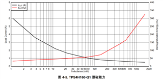
I have another request, could you please provide us with the demagnetization capability curve of TPS2HB16, just like the following image? We need these parameters for reference when selecting diodes or TVS.
If using an external TVS or diode for inductive demagnetization, the external clamp must trigger before the internal clamp so as to avoid any energy going through the FET.
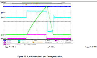
We do not have a similar analysis for TPS2HB16-Q1 but we do have 5mH demagnetization at 13.5V data:
This testing is performed with a 5mH inductor and a low effective resistance. The EN width is triggered in such a way to keep the total energy under the max what the device can handle.
Yeh, this is the maximum amount of energy that the device can dissipate during inductive turn off without damage for both single pulse and repeated pulse. Do note that the energy in the inductor is less than the total energy that is dissipated in the high side switch.