This thread has been locked.

If you have a related question, please click the "Ask a related question" button in the top right corner. The newly created question will be automatically linked to this question.

TPS55288-Q1: Configuring Output Current Limit

Part Number: TPS55288-Q1
Other Parts Discussed in Thread: TPS55288

I'm having trouble configuring the output current limit on my device (Specifically I'm using the TPS55288RPMR). It seems to limit the current to half of whatever limit I try to set.

Following the recommendations in the datasheet, I'm using a 10mΩ current sense resistor. I know I could change that value to get a similar result, but I'd really like to understand what I'm doing wrong.

I'm currently wondering if I'm just overlooking something in one of the config. registers.

The latest values I'm using for testing are:

VREF LSB (0x00) = 0xF

VREF MSB (0x01) = 0x03

IOUT LIMIT (0x02) = 0x7F

VOUT SR (0x03) = 0x01

VOUT FB (0x04) = 0x03

CDC REG (0x05) = 0xE0

MODE REG (0x06) = 0xA8


I'm choosing to max out the voltage to make sure it's not limiting my current as I work through this problem but will set it accordingly once this is resolved.

With no more than seven registers, I'd like to think I'm setting everything correctly. But I've overlooked things before.

Am I missing something obvious or can you recommend some troubleshooting steps?

  • Hi Nolan,

    According to your register value, the output current limit is disabled on IOUT_LIMIT register. Please enable this bit and have a try, with your current setting, the out current limit would be about 6.35A.

    May I know what is the application here? Can you also share the schematic and layout picture?

    BRs,

    Bryce

  • Bryce,

    The IOUT_LIMIT register is actually being set to 0xFF. The enable bit is being set. I'm sorry. That was an oversight on my part.

    I'm supplying it with 20V. It's drawing about 2.05A and it's outputting 12.19V at 3.212A. 

    Presently I'm just doing load testing. The final application will need to be current limited to 4.5A.

    Here's the schematic you requested.

    TPS55288Schematic.pdf

  • Hi Nolan,

    1. What about the Vout when there is no loading? 20Vout?

    2. Can you share the waveforms of SW1, SW2, Vout and inductor current when you found the output current limit is triggered. Need 10ms/div and zoom-in(5us/div).

    From the schematic, 

    1. Why R15 is DNP? It is used to select mode and I2C address.

    2. AGND is not connected to GND.

    3. Can you also share the layout picture here?

    BRs,

    Bryce

  • Bryce,

    1: Without load, Vout = 21.5V

    2: Waveforms

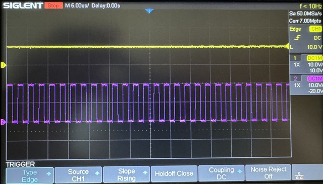
    I'm having difficulty triggering off the FB pin. But the output should saturate the current limit as soon as it hits about 10-12V. So, in the following images, CH1 is VOUT, with a vertical 10V/div and a trigger set to 10V. CH1 is vertically offset by 1 division (+10V).

    I've labeled each image with CH2 the horizontal time/div and the horizontal position. CH2 is also set to 10V/div. CH2 is vertically offset by 2 divisions (-20V).

    SW1 10ms/div, Position -60ms:

    SW1 5us/div, Position 0ms:

    SW2 10ms/div, Position -60ms:

    SW2 5us/div Position 0ms:

    I'm not including dedicated images of VOUT because I used VOUT as CH1 in the previous images.

    I'm not sure how to measure the inductor current with an oscilloscope, but will gladly provide it if you have suggestions on how to measure it.

    From the schematic:

    1: R15 is DNP because Table 7-2. on page 17 of the datasheet says that leaving it open will give me the configurations I want. So I marked it DNP as a reminder to leave the pin open.

    2: Page 45 of the datasheet says that GND and AGND are only supposed to connect on the GND terminal of capacitor C27. If I connect them in the schematic, they'll connect everywhere. So, for now, I have a floating AGND net pointing to the GND terminal of C27 as a reminder to connect them in the PCB layout. You should be able to see it in the image you requested.

    Previously I had a 0 Ohm resistor tying GND and AGND together next to C27, but I wasn't sure that was sufficient, so I found a way to overlap them in the PCB layout.

    3: Layout Picture

    I've left the pours un-poured for image clarity.

    On the top layer:

    The left edge of the image is largely a VDD pour except where you see the N$3 net.

    There's a small N$5 pour connecting L3 to the two MOSFETs.

    There's a small N$20 pour connecting L3 and capacitor C24 to pins 21 and 25 of U3 (the TPS55288).

    An ISP pour connects U3 pins 11 and 12 to all relevant capacitors and R8, the current sense resistor.

    An ISN pour connects R8 to the output screw terminal.

    Near the top, there's a small AGND pour connecting all the AGND terminals of relevant capacitors.

    Everything else should be covered by a single GND pour.

    Layer 2 is a solid GND plane.

    Layer 3 has a few visible traces, but is otherwise covered by a GND pour.

    The bottom layer also has a few visible traces, but is otherwise covered by a GND pour.

    Please let me know if you need additional information. Thank you for all your help so far.

  • Hi Nolan,

    Thanks for your detailed feedback.

    From the layout, I have some questions below.

    1. One thing is you mentioned: ISP and ISN connection, recommend to use Kelvin connection for ISP-ISN voltage sensing, otherwise the output current limit accuracy is poor. You can find more about the layout guideline in the app note as below.

    www.ti.com/lit/an/slvaer0b/slvaer0b.pdf

    2. I don't find which output cap is closest to Vout and GND pin, please point it out. The placement is very critical for Boost side power loop, and recommend to put the 0402 0.1uF as close to the Vout and GND pin as possible.

    3. Can you help show the screen-shoot of each layer? From the layout, I think it was the ISP-ISN connection causes the output current limit problem. You can use one differential voltage probe to test ISP and ISN pin, and see if it equals to the value as you set at the register.

    BRs,

    Bryce

  • Hi Nolan,

    We have not seen an update from you for three weeks, so I assume the questions are answered and the issue is solved.

    I close this thread now. If there is still something open, please reply and the thread will get opened again.

    If you have any other question or of the thread has been locked, please open a new one.

    Clicking the Resolved Button also helps us to maintain this forum.

    Best regards,

    Bryce