Other Parts Discussed in Thread: UCC14141EVM-068
Power Management Forum
E2E Thread Title – UCC14140-Q1: Rlim/RDR selection and thermal issues
I am using the UCC14140-Q1 with dual output. The VDD-VEE voltage is 20V, and the COM-VEE voltage is 5V. I noticed that the way the datasheet solves for Rlim conflicts with the method from the UCC1414x-Q1_Calculator_V7.xlsx tool that TI provides. Can you please confirm my selections?
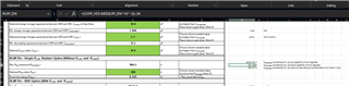
System parameters are below:
Vin: 12V
Cin: 20.1uF (as recommended)
VDD-VEE: 20V
COM-VEE: 5V
Qgtot: 1135nC
Switching Frequency of Gate Driver Load: 20kHz
Quiescent current of gate driver from VDD-COM: 4.95mA
Quiescent current of gate driver from COM-VEE: 6.21mA
Quiescent current of other load on VDD-COM: 0mA
Quiescent current of other load on COM-VEE: 10mA
Bottom feedback resistor between FBVDD and VEE: 10kΩ
Bottom feedback resistor between FBVEE and VEE: 10kΩ
Desired AC gate-switching ripple percentage between VDD and COM: 5%
Max component tolerance of Cout2 and Cout3: +/- 10%
Max Avg Power capability based on provided SOA and Tamb: 1.5W
Max transient power capability based on provide SOA and Tamb: 2.20
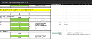
Using my own calculations AND the provided component selection tool, I found that
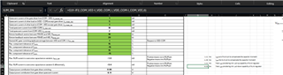
K23 = 2.69
Due to some layout and design constraints, we have opted to select a Cout1b of 0uF, although we have included the recommend Cout1 of 10.1uF near the DC/DC module. Further, we are constrained to a minimum Cout2 of 30uF, and have thus chosen a Cout3 of 90uF.
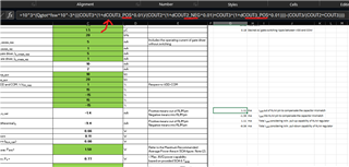
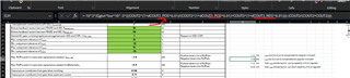
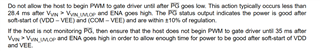
Moving on to the Rlim requirements. I followed the procedure outlined in pages 35-37 of the datasheet for both the single and RDR configurations.
Single configuration:
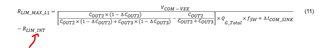
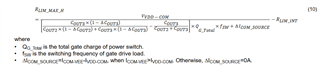
The datasheet indicates that the Rlim in the single-resistor configuration should be the minimum of the results from Equations 10, 11, and 12.
Equation 10:
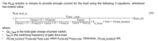
Equation 11:
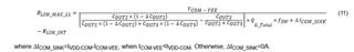
Equation 12:

The discrepancies I have found are as follows:
- Equation 10: for the (1-ΔCout3), the spreadsheet instead uses (1+ΔCout3)
- Equation 11: for the (1-ΔCout2), the spreadsheet instead uses (1+ΔCout2)
- Equation 12: the spreadsheet assumes ΔICOM_SINK is not 0, but in my case, ICOM_VEE>IVDD_COM, so I used a ΔICOM_SINK of 0 (see Equation 11).
In the single resistance case, Equation 12 is the lowest value in both the provided spreadsheet and my calculations, but the aforementioned discrepancy changes the result from 924 Ω (spreadsheet) to 265Ω (my calculations).
In the RDR case, Equation 10 is used to identify RLim1, so the discrepancy in the spreadsheet affects this value as well.
Solving for Rlim2, I used Equation 14:
The discrepancies in Equations 10 and 12 directly affect this calculation. Furthermore, the spreadsheet yields a value for Rlim2 that is significantly higher than that of Rlim1. However, the datasheet indicates that Rlim1 should be significantly higher than Rlim2.
Can you please confirm the Rlim values that I have chosen?
In the single Rlim case, I have Rlim = 266Ω
In the RDR case, I have Rlim1 = 1326Ω, Rlim2 = 299Ω.
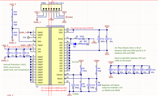
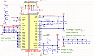
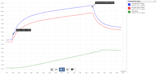
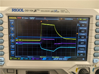
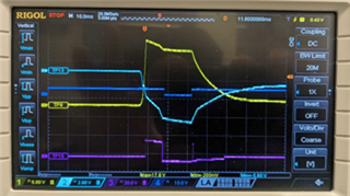
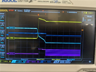
Additionally, I have tried to integrate this DC/DC module into our system using the RDR configuration that I calculated, and I am seeing a very high temperature rise of the module (measured using a thermocouple on the top of the package). Using the thermal resistances provided in the datasheet, I estimate that the package case should only get to about 48°C while switching. However, the case reached over 110°C before I shut down the test, and the temperature was still rising. Further, it seems the steady-state temperature when the gate driver is NOT switching is about 70°C, which is much higher than expected. I am in the process of confirming the quiescent current loading the DC/DC module when the gate driver is not switching, but is there anything else that might cause such high temperature rise? Is it connected to the Rlim and Cout component selection?
Thanks in advance for your help!
P.S. I have attached my personal spreadsheet that I used to follow the datasheet calculation procedures for your reference.