This thread has been locked.

If you have a related question, please click the "Ask a related question" button in the top right corner. The newly created question will be automatically linked to this question.

TPS54560: Split-Rail Power Supply

Part Number: TPS54560
Other Parts Discussed in Thread: TPS54360

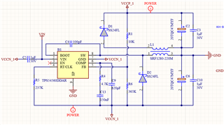
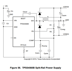
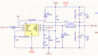
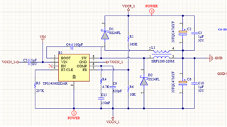
I've designed a circuit referring to the document SLVA369A using TPS54560, it has 24V input and ±15V output. but when I turn the input 24V on, nothing happened. I've compared my design to the document, but I didn't found any difference. The value of the resistor and capacitor is calculated using the SWIFTPOSNEG-CALC-v4.xlsx tool. I'm sort of a newbie to power design, and I really can't find out where the mistake is. Can anyone help me to correct my design? That would help a lot.

  • Hello,

    I will review this and get back to you soon.

    Regards,

    Jimmy

  • Also if you have the calculator tool saved on your end, please attach it for review. 

    If you haven't already done so, please try to power it at no load steady state and I would like the see the following waveforms: VIN, VEN, SW, and FB

  • 7455.SWIFTPOSNEG-CALC-v4.xlsThanks a lot! This is the calculator I used for this design. And I found a mistake in my design: the data sheet says the thermal pad should be connected to the GND pin, but in the split-rail topology, the GND pin is connected as the negative output. And in my design the thermal pad is still connected to the GND net. I should connect the GND pin to the thermal pad together as the negative output. So maybe this is the problem? I don't know if this will affect whether the chip will work correctly or not.

  • Hello,

    Yes this would be impacting the regulation of the device.

    Though the IC's regulation point is referenced to the device's Pin 7 (GND), the thermal pad needs to be connected to Pin 7 for proper operation as noted in the pin description. In your schematic given that Pin 7 (GND) is the negative output rail of the split rail configuration, the thermal power pad must also be connected to the same Pin 7. Dismatch in voltage on both Pin 7 and thermal pad may result in improper regulation.

    Regards,

    Jimmy

  • Hello, I've revised my schematic and connected the thermal pad to pin7, but after power on there isn't any power output (from the screen of the power source I can see a fluctuation of about 0.5A, then it dropped to zero, maybe the current is used to charge the capacitor). There's not any waveform at VIN, VEN, SW, and FB at no load steady state, and the voltage at FB pin is about 0.91V, while VEN is about 5V, Vcomp is about 0.66V. The voltage between the bootstrap capacitor is 230mV. It seems the switch is not operating. Is there anything wrong with my schematic? or which type of working condition may cause this phenomenon?

  • Sorry... I've found out where the problem is. The feedback resistor R1&R6 was reversed, so the voltage at the FB pin was out of range and the regulator doesn't work properly. (A stupid mistake…… orz)

    The correct schematic is put below, in case anyone needs it can have a reference:

    the parameter are as follows:

    input: 18-30V 24V nominal

    output: ±15V 1.3A each

    the calculator is downloaded from: SWIFTPOSNEG-CALC Calculation tool | TI.com

    using device TPS54360(though the calculator doesn't include TPS54560, they are sort of in the same series, different in output current capacity)

    Hopefully it may help.

  • Okay yes that would do it. The feedback resistor is a voltage divider on VOUT to FB and FB wants to regulate to the part's reference voltage.

    Picking the appropriate top and bottom resistor will allow for proper regulation.

    It seems you were able to resolve the issue on your end. I will close this thread for now.

    If you need further assistance, please reply back to this thread and it will reopen for further assistance.

    Thank you for using the E2E forum.

  • Sorry, I've met a further question about the output voltage, my design include dual output (2 TPS54560 supply two ±15V output), the requirement of the sensor voltage is 15V±0.75V. At first, when I only finished the welding of the first chip, the output was relatively accurate, but when I finished the welding of the entire circuit, the output positive and output negative were unbalanced, the positive output was 16V, while the negative output was -14V. the feedback resistor can control the difference between the positive and negative output (the absolute voltage difference between the positive and negative output is controlled at 30V), but fails to control any one of them alone. And if I connect the feedback resistor between GND and the negative output, it can control the negative output to -15V, but the positive output generated by the coupled inductor raised to 19V. 

    My question is, what kind of reason may lead to this phenomenon, is it caused by unreasonable layout or the interference between two chips? Or the selection of the coupled inductor doesn't fit the circuit? And how can I fix it and get a relatively accurate voltage. Thanks a lot.

  • I would suggest on a different board, only populate the two TPS54560 device isolated from other surrounding circuits, power the device at the input capacitors, and load the device at the output capacitors to check regulation and functionality of the dual output rails. If it is okay after this test but then falls out of regulation after the circuiting circuits are populated, then you would need to check what is downstream to the output to cause this regulation.

    If components are not properly soldered onto the PCB then it will cause regulation issues. 

    Please provide waveforms of SW, VOUT+/- and the feedback voltage of the TPS54560 because the device is trying to regulate to this reference voltage.

    Also provide camera image of your application board so I can inspect soldering. 

  • I have not heard back from you for some time so I will assume you were able to resolve the issue on your end.

    If you have any further questions, please reply back to this thread and it will reopen for further discussion.