Other Parts Discussed in Thread: LM5155, , TL431
Hello, we are trying to design a flyback converter with these requirements:
3.3V input, isolated +/- 35V output, ~200kHz switching frequency
The output powers a voltage controlled ~0-2000Hz (AC) current source (using OPA454s...) that needs to deliver up 4.5W.
The transformer we plan to use is the Wurth Electronics 750315839, 1:10:10 winding ratio, 40uH primary inductance, 3.2A saturation current.
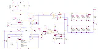
Using the quick start calculator Excel spreadsheet, we arrived at the following schematic:
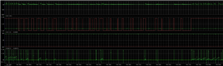
We simulated the circuit with PSpice and got the following results:
The outputs rise to +/- 35V and start to oscillate:
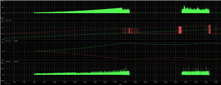
There are also short (~1-2ns), large current spikes >50A when switching on:
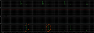
Closeup of the wave form at 248ms, after target voltage is reached:
How can we fix these issues?
The PSpice project and Excel spreadsheet are attached below.
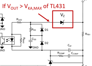
Something else we noticed is that the application note "How to Design an Isolated Flyback Using the LM5155" (SNVA866A), a compensation network is put on both the primary and secondary side (C42, C43, R19, R23 in the schematic above).
In another application note and some forum posts here (which i can't find anymore) it is suggested that the compensation network on the primary side is not necessary. Which one is correct?
LM5157_TRANS-2023-11-09T01-19.zip LM5157_58_Quickstart_Calculator_for_Flyback_Regulator_Design_V1_0_0.xlsx