This thread has been locked.

If you have a related question, please click the "Ask a related question" button in the top right corner. The newly created question will be automatically linked to this question.

TPS2116: TPS2116DRLR

Part Number: TPS2116

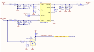
Power switching is performed using TPS2116DRLR. PR1 is set to "H" and VIN1 is used with priority.

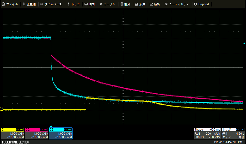
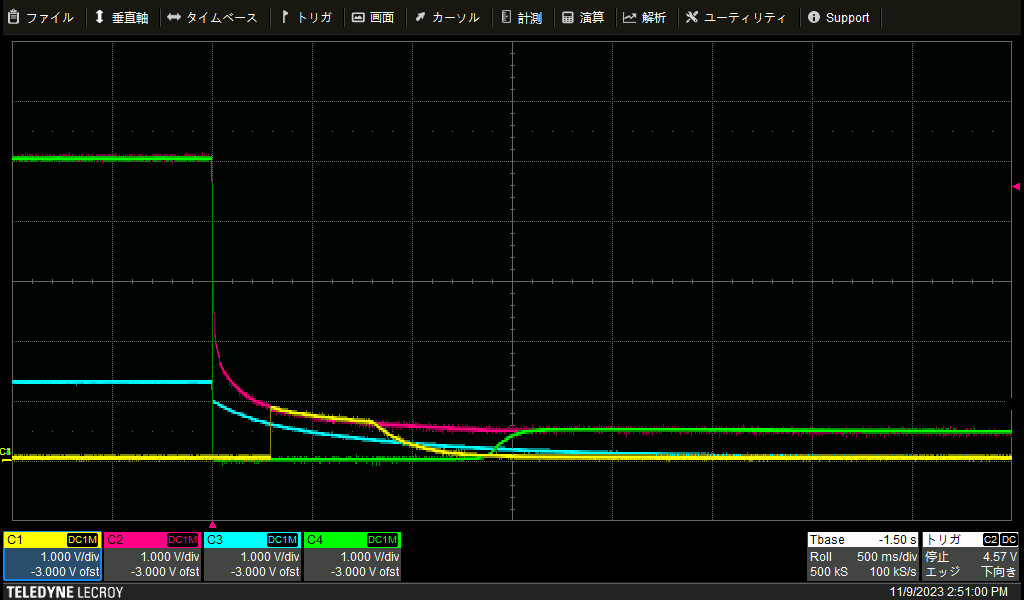
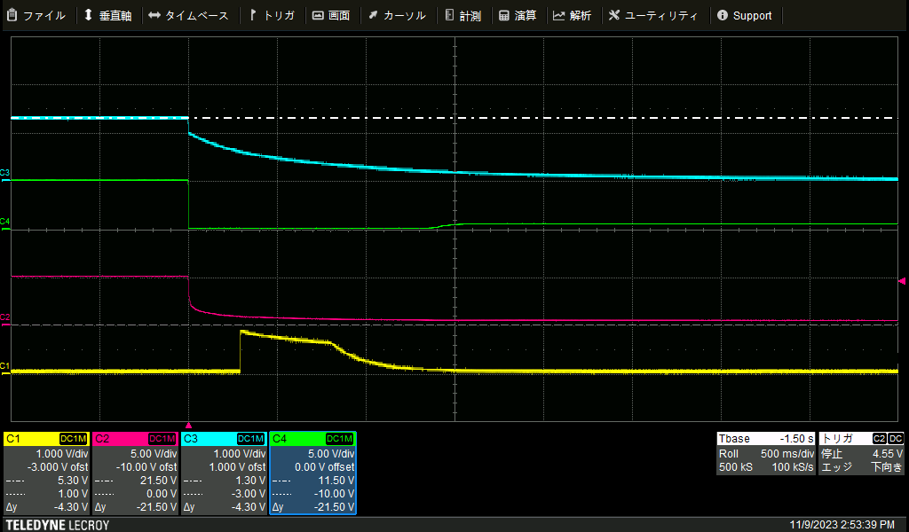
If you turn off VIN1 while using VIN1=5V, VIN2=0V, it seems that the current flows backwards to VIN2.

I understand that VIN1 and VIN2 do not have backflow because they have backflow prevention, but can backflow occur?

1ch=VIN2

2ch=VIN1

3ch=VOUT

  • Hi Azuma-san,

    Welcome to e2e!

    TPS2116 activates reverse current blocking if:

    -VIN1 and VIN2 are below 1.6V

    -VOUT is >44mV greater than VIN1 and VIN2

    -MODE is low and PR1 is high

    Is IN2 held to 0V by a supply or load, or is it floating?

    My initial thought is that PR1 is connected to VIN1 through a resistor divider, and when VIN1/PR1 decrease such that PR1 drops below 1V, the device selects IN2 as the active source. If VIN2 is floating, it will be pulled up to VOUT because there is no load pulling it to GND or enforcing a >44mV difference between VOUT and VIN2 - it looks like this is what is happening in the waveform you sent. Then, when VIN1 drops below 1.6V (with room for tolerances, in this case it looks to be about 1.3V), this creates the condition of having both VIN1 and VIN2 below 1.6V, then the reverse current blocking is enabled and the input channels discharge their capacitance (it looks like there is quite a bit of capacitance in each INx rail) separately from VOUT.

    Do you think this theory applies to your scenario? If not, can you send a schematic and/or a waveform with PR1, VIN2, VOUT, and ST?

    Thanks,

    Patrick

  • Hi Patrick san

    Thank you for your reply.

    Are any of the three items that activate reverse current prevention effective?
    Or do we need all three?
    -VIN1 and VIN2 are below 1.6V
    -VOUT is >44mV greater than VIN1 and VIN2
    -MODE is low and PR1 is high

    My understanding is that if even one of the conditions is met, it will be effective in preventing reflux.

    Since VIN2 is 0V while VIN1 is ON, backflow prevention seems to be effective in that VOUT is >44mV higher than VIN2.
    Now VIN2 is connected to 0V through a resistor (see attached schematic).

    I have confirmed the following items.

    1) Removed R282 connected to VIN2.
    I connected VIN2 to 0V with a pull-down of 1.2k.
    We confirmed that when VIN1 was turned OFF in this state, the current flowed back to VIN2.
    I checked the voltage on the opposite side of VIN2 of the resistor R282 that I removed, but it remained at 0V. Therefore, there is no wraparound from other circuits.

    I attach a waveform with PR1, VIN2, VOUT, and ST.

    1ch=VIN2

    2ch=VOUT

    3ch=PR1

    4ch=ST

  • Hi Azuma-san,

    Only one of the three conditions needs to be met, you are correct. One more thing to mention is that when one input is active, the other input always has reverse blocking on.

    The most important question to consider here is: Is USB0_VBUS floating or does it have a strong pulldown to 0V? Because everything that's effectively floating will be 0V, but can be pulled to any voltage by even a weak source.

    Based on the most recent waveforms you sent, I do believe that the hypothesis in my original reply is correct. Thanks for doing the test with the 1.2kOhm resistor to GND on IN2 - the pulldown needs to be stronger in order to allow enough current to go from VOUT to VIN2 (likely on the order of 5Ohm).

    Is this behavior an issue? Is it toggling your USB0_VBUS_CHECK signal?

    Thanks,

    Patrick