Other Parts Discussed in Thread: UCC21550, TINA-TI
Hi team,
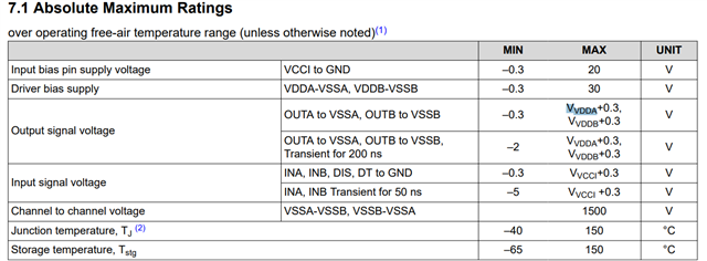
For our datasheet spec, the OUTPUT signal voltage the max value is 'VVDDA+0.3', the VDDA is the real supply value at PIN16, if this understanding is right?
Thanks
Best regards
Mia
This thread has been locked.
If you have a related question, please click the "Ask a related question" button in the top right corner. The newly created question will be automatically linked to this question.
Hi Mia,
Yes, this V_VDDA refers to the voltage at pin 16, and V_VDDB refers to the voltage at pin 11. There is a 2W ESD diodes from the output to each supply to prevent these voltages from occurring, even when the device is unpowered. In addition, when powered, the main output driver usually has a closed NMOS with 0.55 ohms of resistance to VSSA, which also prevents output voltages from exceeding either supply rail. When ON, the PMOS has about 5 ohms to VDDA.
This spec mostly indicates that applying a voltage to the output will forward bias protection diodes and start to cause abnormal behavior, such as powering the VDDA rail through the OUTA-VDDA protection diode. Also, the ESD diode can be shorted by excessive current, which will prevent the output stage from working normally.
Best regards,
Sean
Hi Sean,
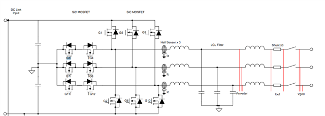
We are using UCC21520 with isolated power rail driving this T-branch G3 and G4.
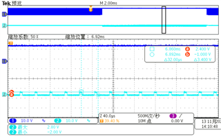
But we find out that there is very large switching spike during G3 normally on status as below:
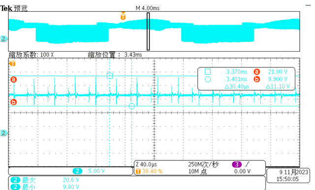
The waveform is captured with 100MHz BW.
If this spike will lead to a damage, any suggestion here?
Thanks
Best regard
Mia
Hi Mia,
You should use the UCC21550 which has a protection feature for output overvoltage. The UCC21520 does have a higher failure rate when exposed to overvoltage.
I don't see G3 labeled on your schematic. When the output of the gate driver is "ON", there are still spikes up to 21V? Where are these spikes coming from?
It looks like these are high frequency spikes without a lot of power behind them. Maybe Miller charge injection?
Can you share your gate drive circuit schematic? You might be able to filter these spikes by adding passive components on the gate drive loop.
Best regards,
Sean
Dear Sean,
The voltage spike, which is evident when Q3 is normal on, is a result of the miller charge caused by the complementary switch switching.
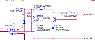
Kindly refer to the following schematic, where the power rails of VCCD_Netural and -2.4V_Netural are powered by an isolated transformer.
The waveform shared by Mia represents the voltage between the gate of Q106B and the ss pin.

BR
Asher.
Hi Asher,
You could try swapping SMF19 with a tighter clamping voltage version like SMF17A or SMF16A. The difference in standoff current will be minimal until the breakdown voltage.
Did you already tune your gate snubber to the spike's resonant frequency? I cannot make out the resonant frequency from the oscilloscope image. A lower resistor than 20 will reduce the spike amplitude, even if it reduces the damping.
I don't understand the function of C135B. It looks like it will disable the PNP turn-off. This might increase the impedance of the OFF output state.
Best regards,
Sean
Dear Sean,
Your suggestion is appreciated. I'll ask our vendors for additional samples and run more tests accordingly.
With regard to item 2, I intend to carry out testing using a lower resistor. Could you please share any calculation documents to help me calculate the resonant frequency?
In our opinion, C135B is beneficial to reduce the maximum positive miller voltage spike.
As a reminder, our initial concern is whether the high voltage spikes caused by Miller charge can cause damage to the UCC21520 since we have already damaged a lot of UCC21520.
The common phenomenon for the damaged IC is the impedance between OUT and VSS is lower than the normal device.
The impedance between OUT and VSS for normal IC: Approx. 0.888Mohm
The impedance between OUT and VSS for damaged IC: Approx. 0.523Mohm
CH2 indicates the test results for the damaged channel, while CH1 shows the normal channel.
BR,
Asher.
Hi Sean,
Want to add some addtional question here and pls help to share some comments:
Q1: Based on the damged abnormal resistor value, could we know the IC do damaged because of the over abs rating of Vvdda?
Q2: Echo to Asher, for the RC snubber, if they follow with fomula 1 in this AN(https://www.ti.com/lit/pdf/slla385) will be okay?
Q3: Going through UCC21550, there is no difference in the ABS rating and the ESD structure, May I know the enhanced output overvoltage protection feature is referring to which function.
Thanks
Best regards
Mia
Hi Mia and Asher,
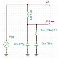
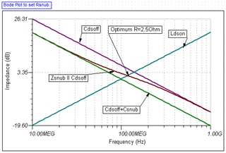
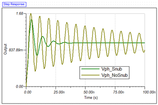
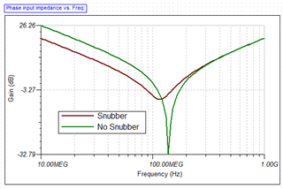
Optimizing the snubber resistor requires you to pick a resistor power rating. Then, calculate the snubber capacitor that will stay within this power as it is cycled at f* CV^2. Then you must calculate the parasitic capacitance and inductance from the d(resonant frequency) with the added capacitor. Finally, you can use TINA-TI to create a bode plot with these values, and you can tweak the resistor value to create the most resistive load possible to intersect with the parasitic inductance. This will give you a more optimized value than the guide.
The IC cannot be damaged by these transients. It has a low-impedance output. These high frequency voltage transients only are detected because there is some series inductance between the low-impedance output on the chip and the point of measurement.
The UCC21550 has an internal protection feature that detects output current and will hold the output state until the output current is below a safe value. This prevents internal inductive kick back from damaging the output transistors.
