Hello ,
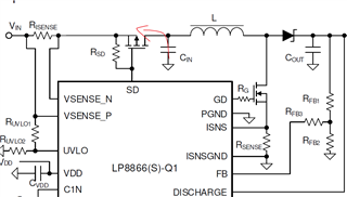
the datasheet and EVM both suggest that the electronic capacitors need to be placed between inductor and P-MOS, right?
- if is possible to move to the input side, before the shunt resistor? How much impact does this design have?
- how to protect the P-MOS? such as add a zenor between G and S electrodes or a normal diode in Drain electrode?