This thread has been locked.

If you have a related question, please click the "Ask a related question" button in the top right corner. The newly created question will be automatically linked to this question.

BQ76952: I2C communication fail when initiation,SCL Level was clamped

Part Number: BQ76952

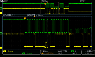
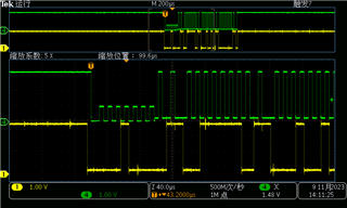
Hi,TI team, we use BQ76952 to design a BMS For 48V battery, and confirm that this chip is the default I2C without CRC. After the overall power-on, we send 0x10 read command to the chip by simulating I2C communication through IO port, and no ACK response is found. Even the SCL level was clamped to about 1.1V in the first few cycles (the chip power supply was 3.3V), and it was found through the simulation device that the single-step simulation showed that the clamped cycle time was variable, sometimes 3-4 clock, sometimes longer, but after that the SCL output level was normal, and no rule was found in this multiple tests. Repeat sending 0x10 for many times and there will be an ACK at some time. However, SCL will be lowered again when the following steps are followed by writing the address of the register that you want to operate, and no ACK response has been checked

the chip wake-up state. During the communication process, the REG18 waveform is measured synchronously and the level is maintained at about 1.81V.

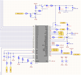
The schematic design is as follows:
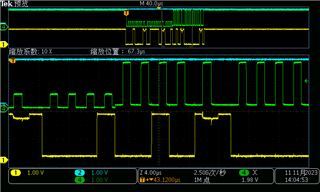
CH1:SDA   CH4:SCL

The following is the 0x10 write exception:

In the following figure, an ACK is available after send 0x10, but subsequent exceptions occur

  • Hi, 

    I notified the I2C bus pull-ups are connected to a +3p3V_D net, but not to the REG1 of the BQ76952. You mentioned the REG18 waveform is power and regulated at all time.

    • Can you also confirm the REG1 and +3p3V_D net are also up the whole time? 
    • Can you share the +3p3V_D portion of the schematic?
    • In addition to the BQ and the MCU, is there any other peripheral connected to the I2C bus? 

    Regards, 

    Arelis G. Guerrero 

  • Hi Arelis

        Thanks for your reply, First, I measure the volt of REG1, that is always 0V, and BREG and REGIN are also 0V during communication. Follow the Technical documentation,REG1 LDO is disabled at BQ76952(BQ76952 15w 4G CVQL)

        Second, I confirm the 3.3V_D is keep 3.3V during communicaiton. Finally, there isn't any other periheral at I2C bus

        what can i do for the REG1 up when device wake up?Look forward to your reply.

    Kind Regards,

    Zhiwen Chen

  • Hi Zhiwen,

    This looks very odd. Could you take these same waveforms again but including the 3.3V_D waveform as well?

    Also, since the issue is with the clock, it may be a problem with the MCU.

    One last thing, you may want to check for any accidental shorts on the board.

    Regards,

    Max Verboncoeur

  • Hi Max,

    This is new waveforms with 3.3V_D(CH2,blue), it stay 3.3V when communication. I have also suspected that the MCU is faulty, but the MCU is only configured as GPIO, it can only output high(3.3V) or low levels(0V), can not output 1.1V, so I think it's probably not about the MCU.

    I tested it with other boards and the results were the same, whereas I'll check the board for shorts

    Kind Regards

    Zhiwen Chen

  • Hi Zhiwen,

    Your schematic doesn't seem to have any issue, and I've never seen the BMS device do this. You may want to confirm that there is no issue with the board itself or with the MCU, as the MCU is the source of the clock signal. Although it's unlikely this is the cause, one thing to check is that the MCU supports clock stretching; this is one of the most common I2C issues I've seen. 

    Regards,

    Max Verboncoeur