A related question is a question created from another question. When the related question is created, it will be automatically linked to the original question.
If you have a related question, please click the "Ask a related question" button in the top right corner. The newly created question will be automatically linked to this question.
Thanks for reaching out. We have several tools available. For a tool specifically made for the LM5157 used in a SEPIC topology, you could take a look at the LM5157 SEPIC Quickstart Calculator.
Furthermore, if you'd like to take a look at a more general tool, that could be used for virtually all power topologies, you could take a look at Power Stage Designer.
Thanks for the feedback. I've found an application note that goes into the basic calculations necessary for SEPIC design. Furthermore, this is the user's guide for the LM5157 SEPIC evaluation module.
If you have certain specific values in mind that you'd like to receive calculation help with, please let me know.
You're very welcome. Could you please attach the filled out quickstart calculator, with these values I can help you design and explain the various parts of the circuit.
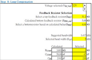
Thanks for the feedback. In Fco you can enter the suggested bandwidth, located right above it.
Then you can use the calculated values for Rcomp/Ccomp/Chf and enter them in the 'selected' column on the right. This should be a good theoretical starting point for the tuning of your compensation loop. But the actual tuning should be done in the lab, since the component placement and PCB routing influences the actual behavior of the system.
To answer your previous question, the suggested bandwidth is most often calculated in a few possible ways: Either the switching frequency divided by 10 or another value. Or the right-half-plane zero divided by 3 or another value. Or the gain-bandwidth-product of the error amplifier divided by 100 or another value.
Perhaps using the frhpz value setting in the converter for bandwidth might be a better approach, but what is the reason for setting the RC compensation in the loop? What impact will not setting it have on the circuit?
setting the RC on the COMP pin configures the poles and zeros for the feedback loop. This, when properly done, ensure the stability of the power stage.
Otherwise the power stage might be not stable, can start to oscillate and worst case get damaged.
OK,So To ensure circuit stability, I need to configure Rcomp, Ccomp, and Chf.
Would different converters have different solving formulas?
Do I simply need to follow the formulas provided in the 'How to Design a Boost Converter Using LM5157x, LM5158x' document to calculate Rcomp, Ccomp, and Chf?
Thanks for the reply. It would be a good assumption to start using the values that are calculated in the Quickstart Calculator. Otherwise you could use the documentation that TI has published for the LM5157-Q1.
But like I said before, these are purely theoretical values and the actual tuning should be done in the lab, since the component placement and PCB routing influences the actual behavior of the system.
There are recommended bandwidth values in Excel. Do I need to set the values smaller than each other?
In addition, should the value of compensation RC be set smaller than the recommended value?
Finally, could you please tell me how to verify that the bandwidth meets the design value through circuit simulation, and is the compensation RC setting correct?
if you study the document I suggested above, you will see that for stability a Phase and Gain Margin should be ensured.
There are some variance on what is recommended but this is also something the user can decide how the environment and what margin he would like to set.
We recommend a phase Margin of > 60 Degree and a gain margin of at least 12dB.
The suggested values are just recommendations. You can adjust them and see the result in the graph on the right side.
To check this, the best is to measure on the real board with a vector network analyzer as this will also capture all the parasitic of the components and the board.
Therefore, we can only use EXCEL to calculate the preliminary compensation RC first, and then conduct actual measurements to confirm whether the phase margin and gain margin are OK, and adjust the most suitable compensation RC.
this depends on the vector network analyzer and is typically in the range of 10 - 50 Ohm. So please check on the used measurement tool what they recommend.