This thread has been locked.

If you have a related question, please click the "Ask a related question" button in the top right corner. The newly created question will be automatically linked to this question.

LM5012: Big ripple on output

Part Number: LM5012

Hi all

I'm designing step-down converter with LM5012. Convert 48V input to 12V output

I using WEBENCH to generate design as below
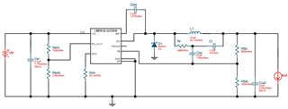
  

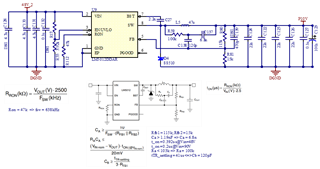
and have PCB with schematics as below (note that C139 wasn't fitted)

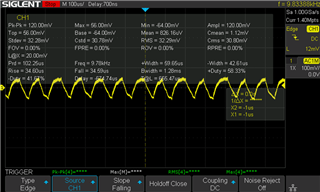
But it have big ripple, about 260mV pk-pk, ripple on scope as below
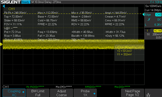
After that, I solder C139 with 22nF, (some others buck converter recommend fit this cap, but LM5012 not refer to this cap in the datasheet) and the ripple reduce significantly, to 32mV pk-pk, as below
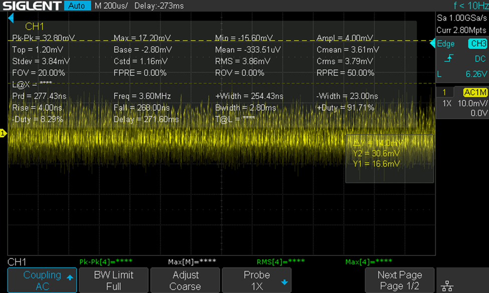
But this circuit ran into problem after few week, that is, output voltage not reach to 12V, about 4V- 5V. however, when I take out C139, voltage recovery to 12V and every thing work ok (except the big ripple as mention above)

So, any one know the root cause of this issue? how I can reduce the ripple when not have C139 (because this cap isn't on the example design in datasheet)

  • Hi Dinh,

    Thank you for sharing your schematic and scope shots. Can you also please send your test setup and the way you are conducting your measurements? This will give us a better understanding of your situation and how best to assist you.

    Thank you,

    Joshua Austria

  • Hi

    I measure by oscilloscope with very short stub of probe, the probe was soldered directly to 2 pin of output capacitor (C124), AC coupling mode. 

  • Hi Dinh, 

    Thank you for sharing your measurement technique.

    Generally when measuring output voltage ripple, TI recommends implementing a tip and barrel method of measurement to ensure insulation to most noise. Proper measurement techniques allow us to minimize the amount of outside noise that might make their way to the measurement. The tip and barrel method also reduces the inductive loop that may come from a long probe ground loop. Please measure your first design with this method. For more information on this type of method you can try this link that I often find helpful: Tip and Barrel Method

    Please let us know if you have any other concerns,

    Joshua Austria

  • Hi Joshua.

    I believe that my measurement technique is correct. The main problem from the circuit. Do you have any recommend on my design?

  • Hi Dinh,

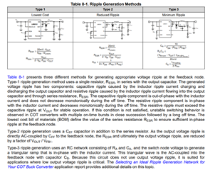
    Thank you for checking your measurement technique. In terms of your design, generating ripple for the LM5012 is outlined on Table 8-1 of the datasheet and in this app note. I have included the excerpt from the datasheet for your convenience:

    I would begin by ensuring that your design fits within these equations. After ensuring that your circuit fits these equations, I would begin to optimize my ripple filter with the app note.

    Hope this helps,

    Joshua Austria

  • Hi Joshua

    Thanks very much for your reply.

    I have made change to my circuit and confirm that all value fit equation. My schematic as below

    and I got ripple as below

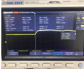
    I have tested for few day. and another issue has rise, that is output volage some time step up very large. as below

    It make all my load die due to over voltage. This is more dangerous than ripple issue. And I have no idea about that.

    it happens very rarely. (3, 4 times in 6 day test and difficult to reproduce). 

    Please recommend me a fix. Now I don't think about ripple any more because at least it don't damage my circuit.

  • Hi Dinh,

    Please send your layout so that we may better assist you. Additionally, please send a scope shot of this behavior with the following probe points:

    VIN

    VOUT

    SW

    FB

    Thank you,

    Joshua Austria

  • Hi Joshua, thanks for your respond

    here is my layout: https://1drv.ms/f/s!Ao2WcIDxKUWtk9INLGxswXyfNBcV7w?e=i2WxCa

    Because it happens very rarely and difficult to reproduce, I will send you scope shot later when I have it.

  • Hi Dinh,

    Please send a screen shot of the layout files instead if possible.

    Thank you,

    Joshua Austria

  • Hi Joshua,

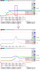
    Finnaly, I found the way to reproduce this issue.

    I happen when the input voltage not stable at the power on moment

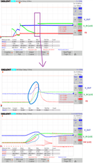
    Here is scope when it occur (just have 3 probe so I only measure SW on 3rd shoot)

  • Hi Joshua,

    the link above already contain a word file that have sceenshoot.

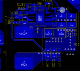
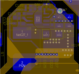
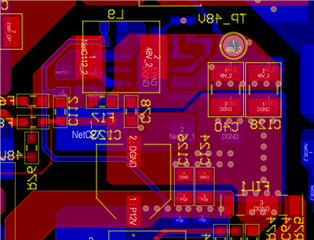
    any way, here is the screen shoot

    Layer 1


    Layer 2: GND

    Layer 3: no signal

     Layer 4:

  • It seem that when Vin drop, LM5012 open large duty cycle, but when Vin recover, it cannot adap on time and still keep duty cycle large. cause over voltage on Vout. Is any way to prevent that?

  • Hi Dinh,

    Thank you for sharing your schematic and layout. 

    After looking through your layout, here are some things I noticed:

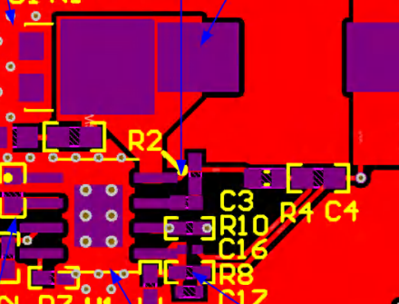
    TI recommends routing the trace that connects the feedback resistors to the output voltage away from the SW node. I believe in your schematic, this is the trace from R80 to C125.- Routing this trace too close to the SW node can contaminate the feedback signal and cause instability in the output voltage. Here is an example of the trace routed away from the SW node:

    It can also be helpful to route this trace on a different layer than your inductor, SW node, and VIN, so the ground plane on layer 2 can help shield the trace from the SW node.  

    I also noticed that you have some VIAs to ground that are placed in the middle of the SW polygon. This would not be advised as this can cause noise coupled into the GND plane that is meant to shield your sensitive traces and increases the size of your SW node.

    Additionally, if D4 can be moved closer to the inductor, you can further decrease the SW polygon area, which may help reduce SW noise and reduce capacitive coupling.

    Please make these changes and see if the results are improved. If you have any more questions in making these, we would be happy to help. 

    Thank you,

    Joshua Austria

  • Hi Joshua .
    Thank you so much for the very detailed recommendation.

    I will make that change in the next version.

    I still have questions about the scope shoot above. That is, when Vin increases, V feedback also increases, but LM5012 still keeps a large duty cycle, so it makes a very big overshoot in Vout, (it should reduce duty cycle immediately when Vin/V_feedback increases). Is there something wrong? How can I prevent this overshoot in next version?

  • Hi Dinh,

    I believe the feedback signal is coupling in noise from SW which is causing this output voltage issue. Can you take a scope shot of the FB and SW pins with this behavior, and we will be able to best see this. 

    Thank you,

    Joshua Austria

  • Hi Joshua.

    The image above is scope shot of FB signal that measure directly on LM5012 pin and SW on the pin of inductor.

    I will take all signal on LM5012 pin and revert to you soon.

  • Hi Dinh,

    I just wanted to let you know that Josh is on Timebank, but should be able to support you when he gets back in the new year.

    Thanks,

    Andrew

  • Hi Dinh,

    Thank you for your patience. It is a little difficult to see from your scope shots, so it would help to see these signals together and zoomed in. 

    Thank you,

    Joshua Austria

  • Hi Joshua.

    I have measured directly on the pin of LM5012 and the results are the same.

    Because this issue occurs when input power is unstable when it is up, so I decided to solder R55 in the schematic above, and add a capacitor parallel with R55 to delay the start up of LM5012 (the purpose is to just enable LM5012 when input power is stable). The problem seems solved.

    So I already updated it on the next version (beside your recommendation about layout above).

    Thank you very much for your support.