This thread has been locked.

If you have a related question, please click the "Ask a related question" button in the top right corner. The newly created question will be automatically linked to this question.

LM5116: LM5116 PCB desgin

Part Number: LM5116

Hello,

Based on the TI user guide for PCB stack-up designing for LM5116(www.ti.com/.../snva285) I defined 4 layers of PCB for it with these features (2-ounce copper top and bottom, 1-ounce copper internal layers on FR4 material with a thickness of 0.06 inches),


I want to know if is it good to a stack-up layer like below:
Top: signal ( I created some fill zones based on the PCB layout template in the datasheet )
Inner 1: GND
Inner 2: 24VDC ( I designed a buck converter with 40 to 60volt input and 24volt with 3.5 A output)
Bottom: signal ( I covered it with a fill zone that connected to the GND net)

Also, currently, I connected PGND and AGND to GND in PCB. Is it right?

Thank you
Leila
  • Hello Leila 

    Please refer my comments below.

    • Fill the unused area on Inner2 with ground coppers. 
    • Use a dedicated AGND copper on the top layer and connect signal components to there.
    • Connect CS-CSG traces to Rsense using kelvin-connection. 
    • Don't connect CSG and DEMB directly to the PGND pin or EP/DAP, but connect them directly to the ground connection of Rsense.  
    •  Populate a small ceramic capacitor between the drain of the high side MOSFET and the ground connection of Rsense. 

    -EL

  • Hello EricLee,

    Thanks a lot for your quick reply and your comments.

    I tried to apply your comments, but I am confused about some of them.
    First (dedicated AGND copper on the top layer): Do you mean I create an AGND fill zone in the top layer?
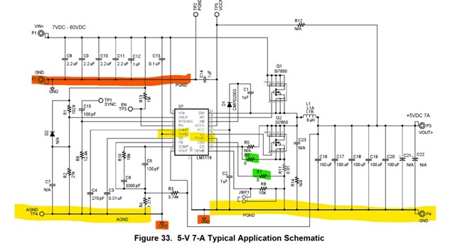
    In the typical schematic in the datasheet of LM5116, PGND, and AGND are connected together and then connected to GND. Then in the PCB layout, we have just net as GND.

    2. kelvin-connection: if you mean using a kelvin-connection is 4-wire or Kelvin sensing measurement around Rsense. Therefore I need to add R5, R6, R7, and R8 in my circuit( based on typical schematic).

    3. Thermal via : is it right connect all of them to GND? 

    At the end, can I initial the stack-up layer like below because I think this setting is better for the return current pass?

    Top: signal
    Inner 1: AGND
    Inner 2: PGND
    Bottom: signal ( I covered it with a fill zone that connected to the GND net)

    Best regards,
    Leila

  • Hello Leila 

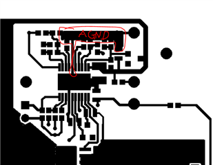
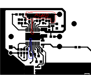
    1. Please refer https://www.ti.com/lit/ug/snva226c/snva226c.pdf . Please find the the AGND copper area circled in red. 

    2. Please use just two wires. One for CS and the other for CSG. Please route them in parallel. Connect them to the Rsense. Please don't connect to other grounds like as PGND/EP..  

    3. Yes, please connect all thermal vias underneath the IC to ground. 

    4. Typically, the AGND copper is located on the top layer and the size is not so much big. Please refer the copper area which I circled in red.  

    -EL

  • Hello EricLee,

    Many thanks for helping me.

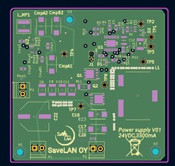
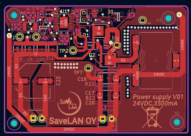
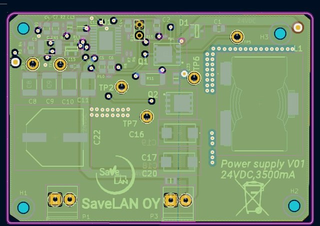
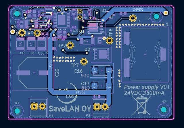
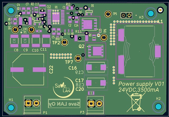
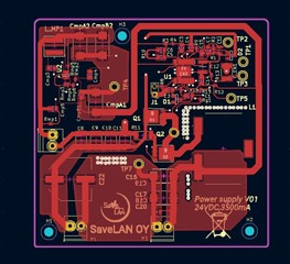
    I tried to apply your advice to my PCB design . On the other hand, based on the mechanical design of the product I had to decrease the size of the board. I hope that I have created the correct Kelvin connection.

    Thank you for your kind advice in advance!

    Best regards,

    Leila

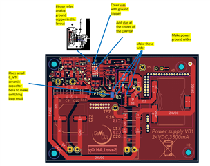
  • Hello Leila

    • Use a dedicated AGND copper on the top layer and connect signal components to there.
    • Connect PGND pin directly to the DAP 
    • Place multiple ground vias underneath the IC. 
    • Don't connect CSG directly to PGND
    • Route L-PGND in parallel. 
    • Route HO-SW in parallel 
    • Place HB capacitor close to the IC
    • Place VCC capacitor close to the IC
    • Power ground coppers are too thin. 

    -EL

  • Hello EricLee, 

    Thank you for your comments. 

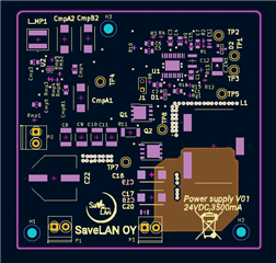
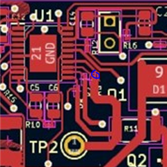
    I tried to apply your comment to my design. But

    The CSG pin by the R6 is connected to the GND of R_Sense(R11).

    Rout Lo and PGND were in parallel at first, but after connecting PGND to GND of R_sense, I had to use a via for connecting to the gate of the Mosfet.

    Rout of Ho and SW were in parallel at the beginning. I tried to keep them in parallel after the Rg1.

    I put 6 vias on the top and bottom of the IC underneath but 3 of them are in the GND zone of IC. Is it right?

    But I have other questions,

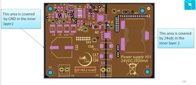
    Is it right to put thermal pads connected to the GND on the top layer? besides, in the 2nd inner layer, this area is covered by a fill that is connected to 24VDC.

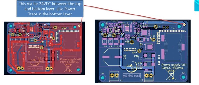
    Also, I am worried about using one via for trace 24VDC between the top and bottom layer.

    Many thanks , 

    Best regards, 

    Leila

  • Hello Leila

    Is it right to put thermal pads connected to the GND on the top layer? ==> Yes

    In the 2nd inner layer, this area is covered by a fill that is connected to 24VDC.==> You don't need. Please cover all unused areas with ground. Actually, I cannot find the 24VDC trace which you mentioned.

    -EL 

  • Hello EricLee, 

    Thanks a lot for your feedback.
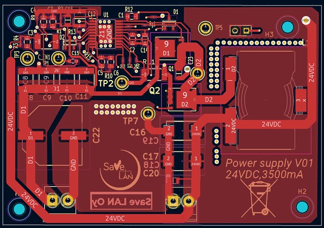
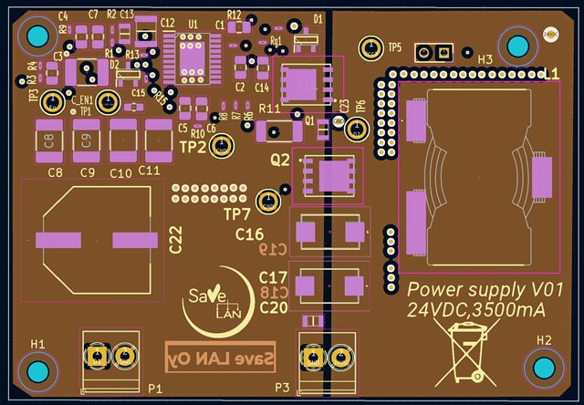
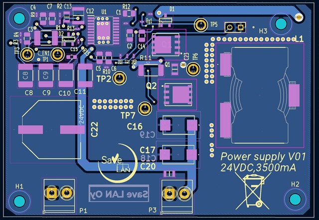
    my meaning about the 24VDC trace is related to one trace located on the right side of the board that is connected by the via between the top and bottom layers.

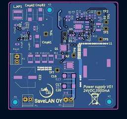
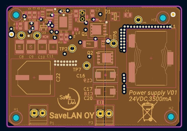
    Also, I put a picture from the inner layer 2 which is divided into two zones, left side GND and right side 24VDC. I am not sure if is it good or not.

    Finnally, about the analog ground, Do you mean that I connect the copper area to the DAP area of the IC ?

    Best regards, 

    Leila

  • Hello Leila 


    my meaning about the 24VDC trace is related to one trace located on the right side of the board that is connected by the via between the top and bottom layers. ==> You don't need such a large VOUT cooper area. Please fill the unused area with ground.  

    About the analog ground, Do you mean that I connect the copper area to the DAP area of the IC ? ==> If you cannot make it sililar with what I showed as a reference , it might be better to connect the analog ground copper area to DAP. 

    -EL