Hello,
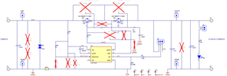
I am using LM74502 in our design as input reverse protection. Below is part of the schematics. In my test, 24V DC is the input voltage, there is no load connected to the output.
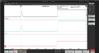
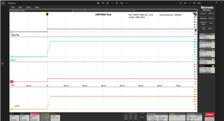
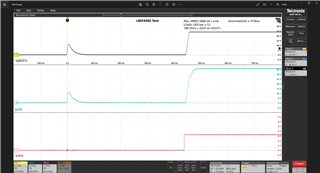
I found a strange behavior on output voltage when powering up. There is a small bump on the output voltage before the output power is fully brought up, as shown in the graph below. "SHDN" signal is connected to EN/UVLO pin of LM74502. From the graph, it shows "SHDN" signal becomes HIGH more than 400ms after that bump on the output voltage.
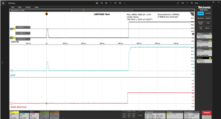
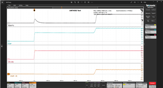
Then, I checked VS, which is the input voltage in our design, and VCAP. It shows that the voltage between VCAP and VS also becomes valid more than 400ms after that bump on output voltage, as shown in the graph below.
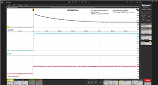
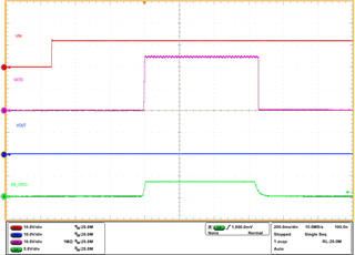
I also measured voltages on GATE and SRC pin of LM74502 as shown below. According to V(GS), the external NMOS should be turned on at our expected time, more than 400ms after the bump. In fact, that bump appears on GATE and SRC pin as well.
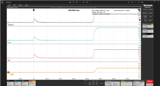
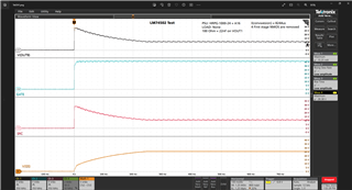
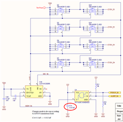
Based on these test results, I believe the charge pump and gate driver of LM74502 work as designed. The bump on output voltage, GATE and SRC pin seems the result of coupling. Have you discovered this phenomenon in other circuits with LM74502 before? Is it possible that the coupling path is inside those external NMOS? Is there a way to solve this kind of problem?
Thank you!