This thread has been locked.

If you have a related question, please click the "Ask a related question" button in the top right corner. The newly created question will be automatically linked to this question.

LM5117: Not outputting signal to the FETS.

Part Number: LM5117
Other Parts Discussed in Thread: CSD19505KTT, CSD19538Q2, CSD18536KCS

I am working with the LM5117 and i have failed to get the output signal to the FETS. 

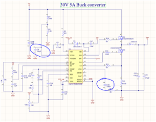
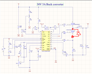
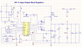
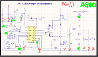
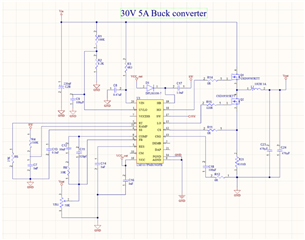
Below is my circuiit diagram with values computed with the LM5117 Quick calc spreadsheet. 

I have measured the following volatges UVLO - 2.5V, RT - 1.2V, SW - 5.3V , VCC - 7.4V, RES, 0V and SS = 0V

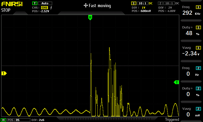
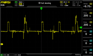
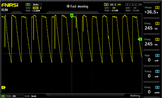
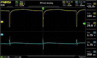
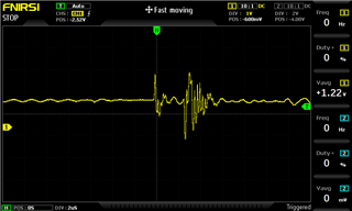
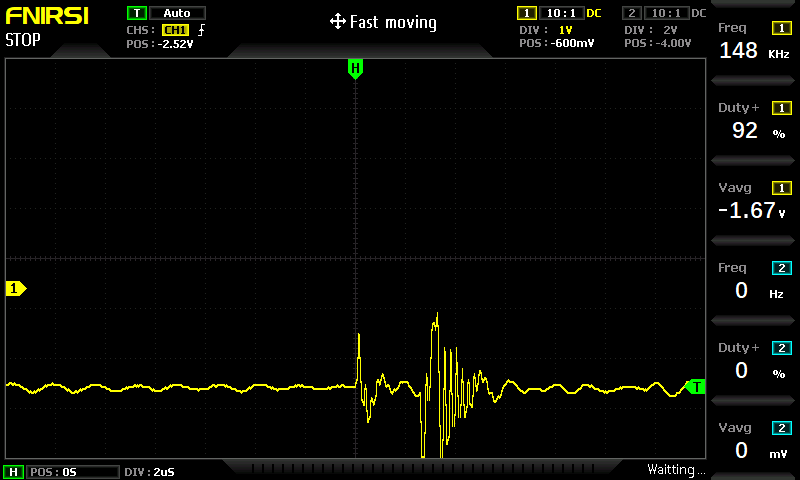
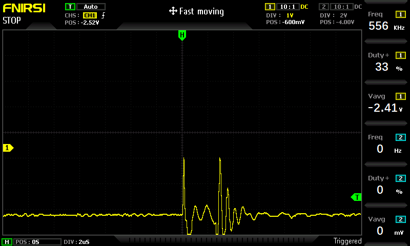
Below are the scope shots showing behaviour at some pins. 

HO

LO

RES

SS

  • Hello Nasser

    Please double check the component values and connections in the blue circles. 

    100uF is too big. C18 shouldn't be populated. 

    -EL

  • Hi Eric, 
    Thank you for your response. 

    I have double replaced C9 to be 120pF and ignore C18 as its not placed but rather has a bridge of solder to complete line to CSG. 

    No cahnge except for the voltage SW is now 0V. 

  • Here is the attached my excel used for component selection buckCalculated values.xls

  • Hello Nasser.

    At first,  please check the VCC pin voltage. If VCC voltage is stable, then check if the SS pin voltage moves up at start-up. 

    -EL 

  • Hi Eric, 

    I have 7.39V at the VCC pin and it is stable, SS pin voltage moves up at startup to 4.3V and its maintained there. 

  • @EricLee , just abit more context .

    It's confusing because my Power supply is set to 30VDC output and its current meter indicates the setup is drawing 0.001Amps, i am inclinced to think the chipset is not switching on. This is on the second pcb is assembled. The first was working untill i ruined the chipset doing some test and teven when i repalced it with several other chips the first board didnt get to work again and i decided to assemble this, a second and its failing to output any bit of signal to the FETS. 

  • Hello Nasser

    Next step is COMP. Please check if COMP moving up when SS increases. 

    1. VCC==> 7.39V and stable

    2. SS ==> moves up at startup to 4.3V

    3. COMP ? 

     -EL

  • Hello Eric, 

    Observation at  COMP pin- OV , no change noticeable at startup. 

    -NK

  • Hi NK, 

    Because of the Thanksgiving holiday in U.S., so I will respond to your questions in the meantime. I check your schematic, and I found you use a adjustable resistance at FB pin. And the COMP voltage is abnormal. Can you check whether the resistance values ​​of the upper and lower voltage dividing resistors obtained by this resistor are correct? Or you can put dividing resistors to replace that (Rfbt=100kohm,Rfbb=2.74kohm). Can you also test the FB pin voltage? Thanks.

    Aurora

  • Hi AT, 

    I have changed Rfbt to 100kOhm and Rfbb =2.7kOhm. 

    SS pin now has 4.6V , Fb pin has  0V. 

    Below is Wave form at Gate pin of highside FET

  • Hi NK,

    From your waveform, the gate voltage seems lower. So it cannot drive your mosfet. Can you try to change R15 to 0ohm? 120ohm is too large for a drive resistor. Thanks.

    Aurora

  • Hello AT, 

    With 35V in i was able to get 30.6V with out load and the ammeter reads 2mA at the input. Afte loading, I still got 30.6v at 2.54A, the ammeter of teh power suppply was still at 35V but indicating current being drawn as 2.1A. 

    This lasted for sometime and later the higside FET smoked. I replaced the FET and still it smoked. Could you share some pointers on where i need to optimise to prevent that, my target is tro draw 5A at 30V. 

    highside fet before the smoking happenend and no load. 

    After the first smoking and i repalced the FETs

  • The output voltage also drops to 16V too. 

  • Hi NK, 

    Can you measure the deadtime between HO and LO single to see if there is any risk of direct access? In addition, the current choice of LS mosfet is not suitable. The reverse recovery loss generated by the LS mosfet is too large, and this part of the loss will fall on the HS mosfet. You may consider replacing the LS mosfet with an Rdson of around 20~30mohm. You can also connect a Schottky diode in reverse parallel to the LS mosfet to see if it helps. You can refer to below table to check the power losses. Thanks.

    Aurora

  • Hi AT, 

    On zooming on the scope images, I can see there is risk for current shoot through. The LS starts to raise to on state 25nS before the HS starts to go low. before connecting the load. 

    Please could you recommend a LS that i can pair up with the current HS. I am thinking about using  N Channel FET  220N06L3, do you think its good subsititute. Kinldy guide on the connection of the schottky diode on LS measured. 

    Thank you. 

  • Hello Nasser 

    Please connect the diode in parallel with the low-side MOSFET.


    -EL

  • Hello Nasser

    This is what I found from DIGIKEY https://www.digikey.com/short/4p149wv4 

    -EL

  • Hi EL and AT, 

    Thank you for teh back and fourthe that we have been having over time. I am still onto this and will aprreciate any extra guidance you will provide to me. 

    Origianlly I had a PCB already done and has not really perfomed well, this is why we have been having this thread. 

    I have made teh decisoin to actually redo anothe PCB , this time round paying keen attention to comeponet selection and the PCB schematics. Having had a challenge with the FET selection on the previous version i have choosen to go in with the actual ones used in the TI evaluation board. 

    I have attached here my new schematics for you to review and guide me while I also work on teh PCB and will also sahre it immediately before I send it for fabrication. 

    I will be most humbled for your review on this. 

    Icomputed Values for BuckCOnverter.pdf

  • Hello Nasser 

    Please refer my comments below. 

    • 150W power supply requires a thermally optimized PCB design to handle the power dissipation. 
    • If hard saturation core, the saturation current of the inductor should be greater than 12.1A
    • >~25V minimum start-up voltage is enough for the 35V minimum input voltage.  
    • Typically high-RDSON low-Qg MOSFET is used on the high-side, and low-RDSON high-Qg MOSFET is used on the low-side. 
    • It is recommended to separate analog ground from power ground on the schematic. 
    • C3 value is too high.
    • D4 direction is wrong. 
    • Use ~1uF at C4 
    • Use ~1uF at C9
    • Adjust loop compensation and make the crossover frequency < ~4kHz

    -EL

  • HI Eric, 

    I have revised the schematics  as in your last response. Notably is my choice of FETS that i wouldlike you to evaluate, they both a TI FET's , CSD19538Q2 on the higside and CSD19505KTT on the low side. 

    I have attached a brief spec sheet of the choice of this is the inductor i will use. 


    I have adjusted the loop compesation to ~1KHZ. 

    I will await your response to kick off on the PCB. 

    5466.Buck Converter.pdf

  • Hello Nasser 

    Please refer my additional comments below. 

    • Separate AGND and PGND on the schematic level, and tie them via a net-tie
    • D2 is unnecessary
    • Use >50V diode at D1
    • Can you select >50V FET in order to make Qg x Rds smaller ? I think you can find a smaller Rdson MOSFET on the high side.

    -EL

  • Thank Eric, Please calrrify on your last statement. I should find a smaller RdsOn Mosfet on the high side, could you tell me what range in mΩ . Also for >50V FET, are you meaning Vds for Highside.  Thank you. 

  • Hello Nasser 

    The smaller Rdson is the better always. 

    Yes, you selected 100V MOSFET while the maximum VIN is only 30V. In general, 50V is enough for 30V application. 

    -EL

  • Thank you Eric, I got you there. I have updated the schematics as dsicussed, i have selected CSD18536KCS on the low side and Replaced teh boot diode with PMEG60T20ELXDX.

    I have not yet connected AGND with PGND , I am curious what I have to consider while making this link, whats your thought on that. Lastly, for the PCB layout shared, the component placing and how i have tried to disspate the heat for the HS with vias to the bottom plane of that net.  is it not risky to disspate heat that heat into the PCB its'self ?

    Thank you. 

  • Hello Nasser

    • Please confirm the maximum input voltage. 
    • Please connect AGND and PGND at the DAP/EP.

    • Yes, there is a risk. If you can, please consider heat-sink on both sides.

    -EL