This thread has been locked.

If you have a related question, please click the "Ask a related question" button in the top right corner. The newly created question will be automatically linked to this question.

LM5143: Selecting MOSFET for Vout 11V- 100A

Part Number: LM5143

Hi all,

My design: Vin 60V, Vout 11V, Imax = 100A, Fsw = 300kHz.

1, I need some helps to select MOSFET for high side and low side. The currently I chose BSC036NE7NS3GATMA1, but when I entered the parmameter into

the quickdesign tool, the effeciency at load 100A is very low.

Please explain more with this.

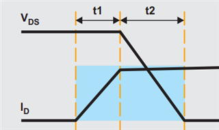
2, Follow the datasheet, the power loss for switching of low-side Mosfet is neglible , I don't understand this.

  • Dao,

    The switching losses is controlled by SW node rise and fall times, this is mostly controlled by high-side MOSFET turn-on and turn-off time.

    The low-side MOSFET dominant losses are conduction losses, especially at low duty cycle and high IOUT.

    The RDSON of the low-side MOSFET is what controls those losses, note they are I^2 * R losses, so they increase exponentially with current.

    Thus it is important to reduce low-side MOSFET RDSON (and inductor DCR).

    You have to have lower RDSON on the low-side FET. Alternatively you can uses parallel FETs to parallel the RDSON.

    Hope this helps,

    -Orlando

  • Hi Orlando,

    My understand that Fsw and tr and tf are same the high-side. So why the switching loss is different, is Vin different?

    As I know, Vin is VDS(off) of mosfet when we calculate the switching loss.

  • Dao,

    HO sources highside FET and controls SW turning on. HOL sinks high-side FET and controls SW turning off.

    Rise and fall times will be similar if HO and HOL are connected to the FET, or use the same gate resistor.

    If you have different gate resistors for HO and HOL then the rise and fall time will be different.

    Yes, VIN is VDS(off) of MOSFET. 

    Note that buck "switching losses" are result of overlaping current and voltage.

    Please reference https://www.ti.com/lit/an/slyt664/slyt664.pdf and figure 5 blue area.

    The high-side MOSFET has to overlap all of VDS / VIN and switching current.

    The low-side MOSFET does not overlap all of VDS with switching current. Low-side MOSFET only overlaps low-side body diode voltage ~0.7V with switching current, so the switching losses are much lower compared to high-side.

    Hope this helps.

    -Orlando