This thread has been locked.

If you have a related question, please click the "Ask a related question" button in the top right corner. The newly created question will be automatically linked to this question.

TPS563201: TPS563201 output not stable and DCM Switch signal overshoot

Part Number: TPS563201

I encounter three problems when I use tps563201.

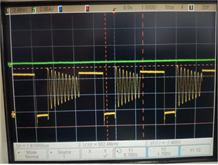
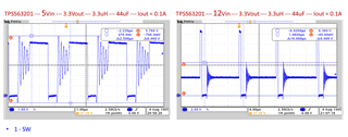
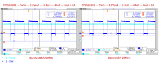
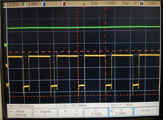
1.When DCM mode,switch node have overshoot voltage.Why? Which parameter should I adjust.

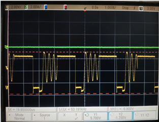
2.When CCM mode,switch node have undershoot voltage.Why? Which parameter should I adjust.

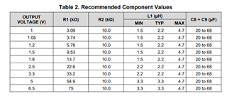
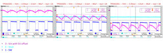
3.Output Voltage Vary with load,when load is 1A,output is 3.34V,when load is 2A,output is 3.29V,when load is 3A,output is 3.23V,Why? Which parameter should I adjust.


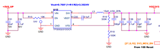
Our schematic is as below,thanks!

  • Hi Yx,

    1.In DCM mode, the oscillation is too large, maybe it's because the inductor too large. Please refer to the recommended value in the datasheet.

    2."When CCM mode, switch node have undershoot voltage. Why? Which parameter should I adjust."  Do you mean the undershoot voltage is too low? I'm not sure what the bandwidth is when you tested?

    3.It seems that FB has been interfered with noise. Please replace the inductor with a suitable one , reduce the resistance of the voltage dividing resistor (as shown below) and then test again. In addition, please provide the layout. I need to check whether the wiring of the layout. 

    Best regards,

    Zhou

  • 1.In DCM mode, the oscillation is too large, maybe it's because the inductor too large. Please refer to the recommended value in the datasheet.

    I changed Inductor to 3.3uH,but no improvement.Waveform as below:no difference with 10uH

    2."When CCM mode, switch node have undershoot voltage. Why? Which parameter should I adjust."  Do you mean the undershoot voltage is too low? I'm not sure what the bandwidth is when you tested?

    I tried 20MHz and 1GHz, -1.7V at 20MHz,-2.3V at 1GHz.

    3.It seems that FB has been interfered with noise. Please replace the inductor with a suitable one , reduce the resistance of the voltage dividing resistor (as shown below) and then test again. In addition, please provide the layout. I need to check whether the wiring of the layout.

    Layout as below:

  • Hi Yx,

    1. In DCM mode, SW oscillation is a normal phenomenon. When Vin=12V, the same phenomenon occurs, but the voltage is relatively smaller due to the larger Vin.


    2. The undershoot of SW is too large in the CCM, which may be related to the measured bandwidth (as shown below: 500MHz Vs 20MHz bandwidth) or the selection of measurement reference ground.


    3. When Iout = 1A, 2A, and 3A, Vout gradually becomes smaller. We can also reproduce it in the laboratory (as shown below). It may be related to the load capacity of the power supply (5V-Vin). It is recommended to measure the ripple of Vin to check.

    Best Redards,

    Zhou